Troubleshooting Solder Defects in PCBA Prototyping
Troubleshooting Solder Defects in PCBA Prototyping
- By: Shuxuan Jiang
- Published: September 25, 2026 |
Modified: September 25, 2026 - Estimated read time: 7 minutes
- By: Shuxuan Jiang
- Published: September 25, 2026 |
Modified: September 25, 2026 - Estimated read time: 7 minutes
- 1. Step 1: Choose solder paste based on your process
- 2. Alloy
- 3. Particle size
- 4. Flux chemistry
- 5. Step 2: Troubleshoot the solder paste application process
- 6. Stencil printing
- 7. Automatic dispensing systems
- 8. Manual application
- 9. Step 3: Reflow, inspect, and rework
- 10. A better way to prototype PCB assembly
- 11. References
- 1. Step 1: Choose solder paste based on your process
- 2. Alloy
- 3. Particle size
- 4. Flux chemistry
- 5. Step 2: Troubleshoot the solder paste application process
- 6. Stencil printing
- 7. Automatic dispensing systems
- 8. Manual application
- 9. Step 3: Reflow, inspect, and rework
- 10. A better way to prototype PCB assembly
- 11. References
People who can reliably hand-solder 0402 components exist. In fact, we have a few here at Voltera. But when a 20-board prototype run involves hundreds of 0402 components, each roughly the size of a poppy seed, surface mount technology (SMT) assembly becomes much less forgiving of small variations in solder paste volume, component placement, and reflow.
“It's mind-numbing, repetitive under a microscope, picking up 0402s with tweezers.” — Hardware Team Lead, technology company
“Even 0402, I just can’t place those properly by hand.” — President, hardware company
In SMT assembly, each step influences the next. Solder paste selection and handling affect deposition quality; the amount and position of each deposit influence how components sit on the board and behave during reflow; and the reflow process ultimately determines whether those deposits form reliable solder joints. In prototype runs, where teams may be assembling only a handful or a few dozen boards at a time, some troubleshooting of solder paste defects is unavoidable regardless of the PCB assembly process.
In a previous blog, we covered common solder paste defects in PCBA prototyping, including missing deposits, solder bridges, solder slump, and solder offset, and looked at what causes them. This blog takes the next step: how to troubleshoot those defects, identify where the process is going wrong, and reduce the chances of them recurring.
Step 1: Choose solder paste based on your process
Alloy
Leaded and lead-free formulations have different melting behavior and reflow requirements, while additions such as bismuth, antimony, silver, and copper can change joint microstructure and mechanical properties. For example, in a study exploring the effect of solder paste alloy on solder voiding, researchers found that Sn-3.0Ag-0.5Cu (SAC305) and SAC-Bi (3.0% Bi) produced the smallest solder voids, while SAC-Bi-Sb (with antimony added) voided the most [1].
Particle size
Solder paste is a suspension of metal particles in a flux vehicle, and finer-particle pastes are used as deposits and apertures get smaller. For direct solder paste dispensing, the particle also has to pass through the nozzle reliably. A useful starting point is a nozzle inner diameter around six to seven times the paste's maximum particle diameter.
Flux chemistry
Flux acts as a flowing agent and a stabilizer, and affects oxide removal, wetting, print stability, residue, and voiding. For example, a study [2] on water-soluble, Type 7 solder paste found a real tradeoff between flux activity, viscosity stability, wetting, and fine-pitch printability: sebacic acid boosts flux activity and printability but degrades stability over time, while suberic acid gives better stability but weaker printability, so the best-performing paste combines both.

If you’re working with the V-One PCB printer, here’s a guide on choosing the right solder paste for your application.
Step 2: Troubleshoot the solder paste application process
Once the material is under control, how solder paste reaches the pad will introduce different sources of variation.
Stencil printing
Stencil printing can deposit solder paste on an entire board quickly, but good results depend on much more than aligning two fiducials. The stencil aperture has to fill and then release the right amount of paste. In experimental stencil-printing research, printing speed, aperture area ratio, and solder-paste particle characteristics were all predictive of the area, height, and volume of the deposited solder paste [3].
In some cases, stencil design can even influence defects that appear only after reflow. In a 2023 study [4], researchers deposited the same total paste volume using different aperture patterns and found that divided apertures produced substantially less voiding in their experimental assembly.
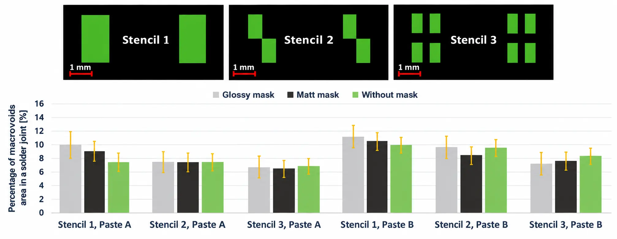
If the same fine-pitch pads repeatedly show insufficient solder paste, don’t push the squeegee harder. Instead, check each potential cause one at a time: aperture dimensions and area ratio, stencil cleanliness, paste condition, board support, and stencil to PCB separation.
Automatic dispensing systems
For stable designs and repeated boards, stencil printing can make sense. For prototypes that change frequently, however, every PCB revision can also mean revisiting stencil tooling and alignment. That's why many teams favor automatic dispensing systems over stencils. Automatic solder paste dispensing systems remove the stencils, but they have their own variables.
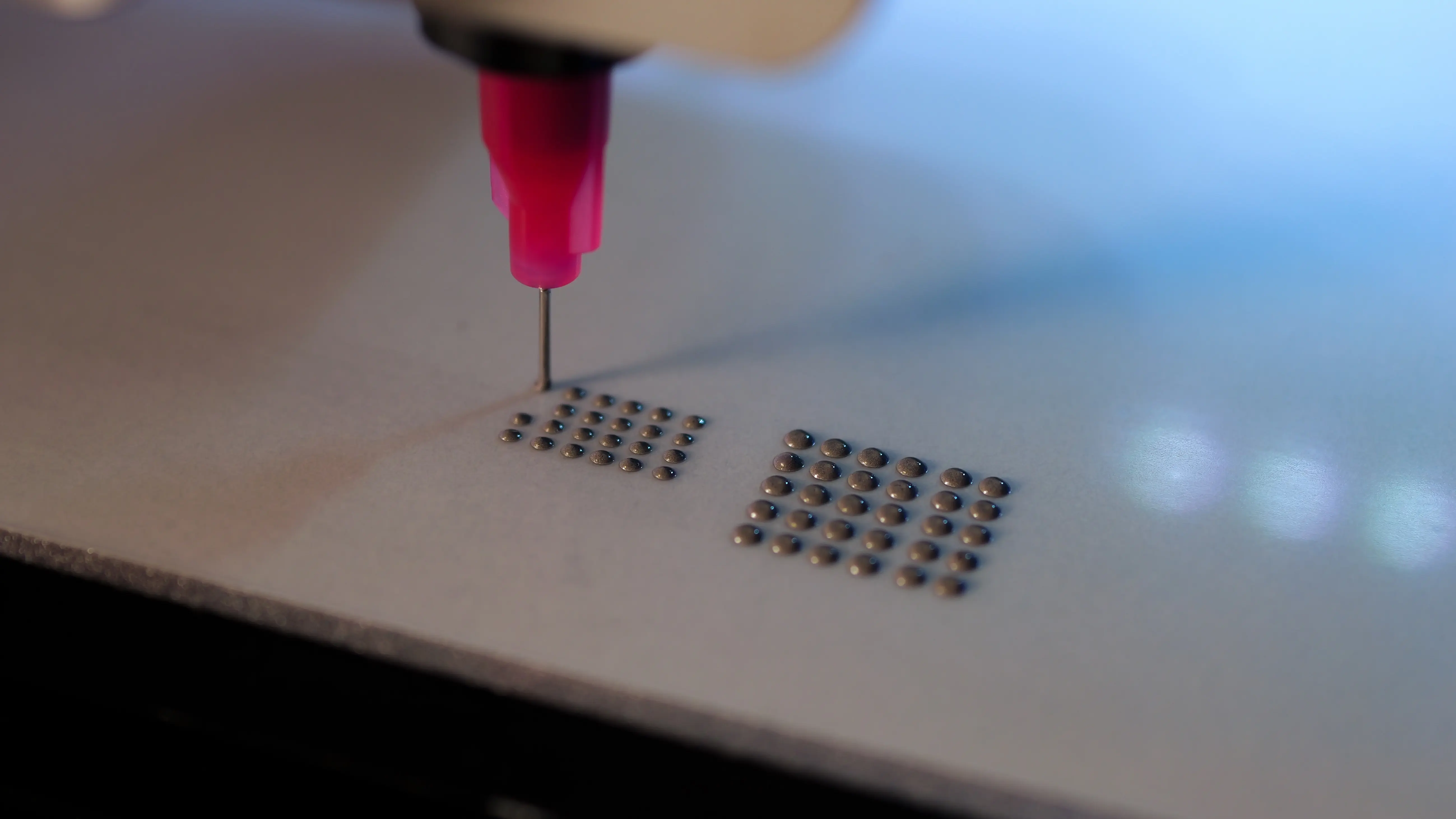
For an automated dispenser, the first thing to look at is the dispensing parameters: nozzle-to-board distance, dispense volume or flow calibration, movement and dwell settings, and, where relevant, actuation pressure or auger speed. Here’s a guide on common dispensing parameters and how they influence the quality of the deposits.
If deposits gradually become smaller, irregular, or intermittent, check the likely causes one at a time: paste temperature, nozzle clogging, paste condition, air in the cartridge, and whether the dispense gap still matches the calibrated Z-height. Paste rheology is time- and shear-dependent, so yesterday's settings are not automatically proof that today's material condition is correct.
Manual application
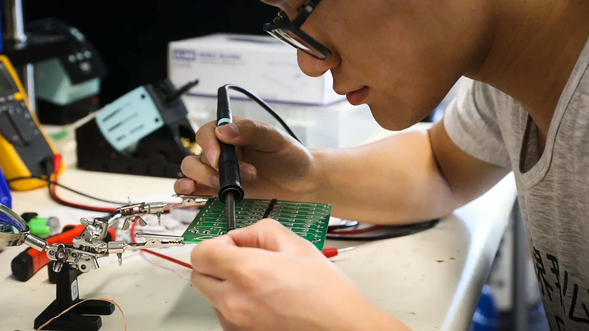
Manual solder paste application is workable for one-off boards, larger pads, or quick rework, but the operator directly controls nearly every variable that an automated dispenser would otherwise standardize: deposit size, placement, start/stop timing, syringe angle, pressure, and consistency from pad to pad.
If hand-applied deposits are too large or inconsistent, start with the basics: use a smaller dispensing tip, reduce the pressure applied to the syringe, and avoid holding the tip in one place too long. If deposits are too small or intermittent, check whether the paste is too cold, beginning to dry out, or difficult to push through the selected tip. For fine-pitch footprints, placing the tip close to the pad and using a repeatable motion helps reduce variation, although manual dispensing will still be more operator-dependent than stencil printing or automated dispensing.
Step 3: Reflow, inspect, and rework
Perfect-looking solder paste can still become a bad solder joint if the thermal process is wrong. A reflow profile controls how quickly the assembly heats, how long flux activation and soaking occur, the time spent above the alloy's liquidus temperature, peak temperature, and cooling. More importantly, the temperature the PCB actually experiences matters. In a 2025 study using experimental data from a forced-convection line, optimization of the reflow temperature recipe reduced the researchers' defect metric by roughly 74-75% and increased pass rate by 2.3% relative to the original recipe [5]. This shows how strongly downstream quality can respond to thermal-process settings even when paste deposition is held consistent.
As such, inspection should happen before and after reflow. Before placement, check whether deposits are present, centered, and reasonably consistent; this is the same principle behind industrial solder paste inspection. A visible solder bridge can often be diagnosed optically but not internal voiding. If hidden solder joints or voids are the concern, reworking the visible surface repeatedly may never reveal the actual problem. It’s therefore important to ask what the failed joint reveals about the solder paste application process, and improve it accordingly.
A better way to prototype PCB assembly
For a new product introduction (NPI) team, the real cost of a solder defect is rarely one bad joint. It is the iteration it interrupts: stop the build, inspect, rework, verify, and then decide whether the result was a random event or evidence that something upstream needs to change.
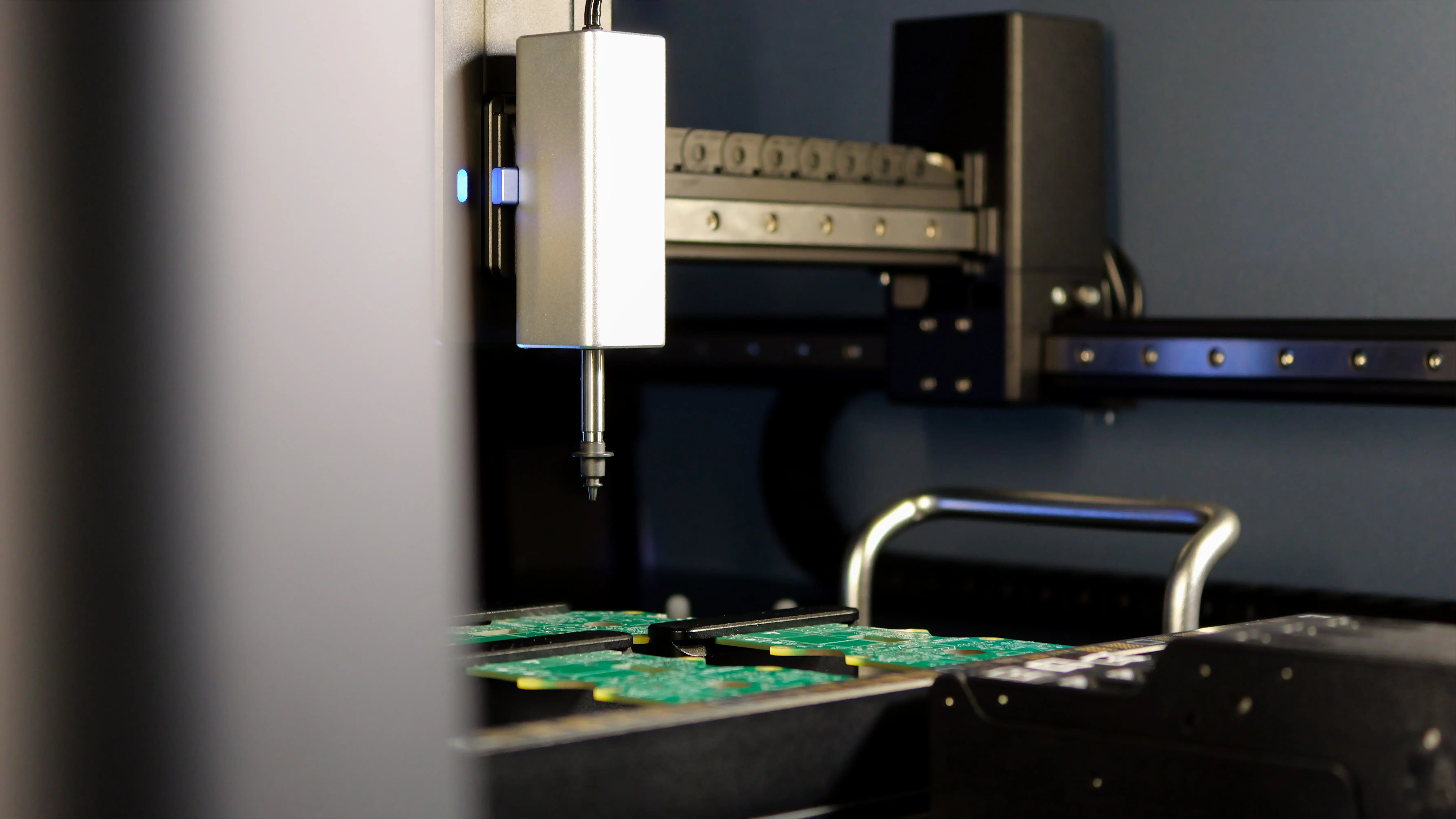
That is where repeatable in-house deposition and placement become valuable. Instead of relying on hand-applied paste for one revision, ordering a new stencil for the next, and manually placing fine-pitch parts after that, Alta keeps more of those variables inside one controlled workflow.
Interested in learning more about Alta? Sign up to get monthly updates.
References
[1] Alakayleh, A., El Amine Belhadi, M., Tahat, S., HMasha, E., Shmatok, A., Alahmer, A., & Hamasha, S. (2023). Effect of solder paste alloy and volume on solder voiding. In 2023 22nd IEEE Intersociety Conference on Thermal and Thermomechanical Phenomena in Electronic Systems (ITherm) (pp. 1–8). IEEE. https://doi.org/10.1109/ITherm55368.2023.10177534.
[2] Choi, D., Park, S. H., Mhin, S., Hong, W. S., & Yoo, S. (2024). Printability evaluation of water-soluble Type 7 solder paste for fine pitch advanced package interconnects. 2024 IEEE 26th Electronics Packaging Technology Conference (EPTC), Singapore, 774–777. https://doi.org/10.1109/EPTC62800.2024.10909844.
[3] Martinek P, Illés B, Codreanu N, Krammer O. Investigating Machine Learning Techniques for Predicting the Process Characteristics of Stencil Printing. Materials. 2022; 15(14):4734. https://doi.org/10.3390/ma15144734.
[4] Kozak, M., Vesely, P., & Dusek, K. (2023). Analysis of solder mask roughness and stencil shape influence on void formation in solder joints. Welding in the World, 67(5), 1347–1355. https://doi.org/10.1007/s40194-023-01505-7.
[5] Li, Y., Zhang, Z., Won, D., & Yoon, S. W. (2025). Soldering reflow process optimization based on simulation. The International Journal of Advanced Manufacturing Technology, 136(7–8), 3163–3176. https://doi.org/10.1007/s00170-024-14944-3.
[6] Qi, M., Yin, T., Cheng, G., Xu, Y., Meng, H., Wang, Y., & Cui, S. (2022). Research on Printing Defects Inspection of Solder Paste Images. Wireless Communications and Mobile Computing, 2022(1). https://doi.org/10.1155/2022/8651956.
Check out our customer stories
Take a closer look at what our customers are doing in the industry.