PCBA Testing Methods: From Prototype to Production
Printed circuit board assembly (PCBA) testing refers to a set of verification methods applied after assembly to detect defects, validate functionality, and ensure long-term reliability. Issues discovered late, especially without precise fault localization, can lead to costly field failures, product recalls, and damage to brand reputation.
Types of PCBA tests in the prototyping stage
Prototype builds typically involve small quantities and rapid iterations. The goal of testing at this stage is to verify that the design functions electrically and to catch major assembly defects early without the expense of production-level fixtures.
Visual inspection and early automatic optical inspection (AOI)
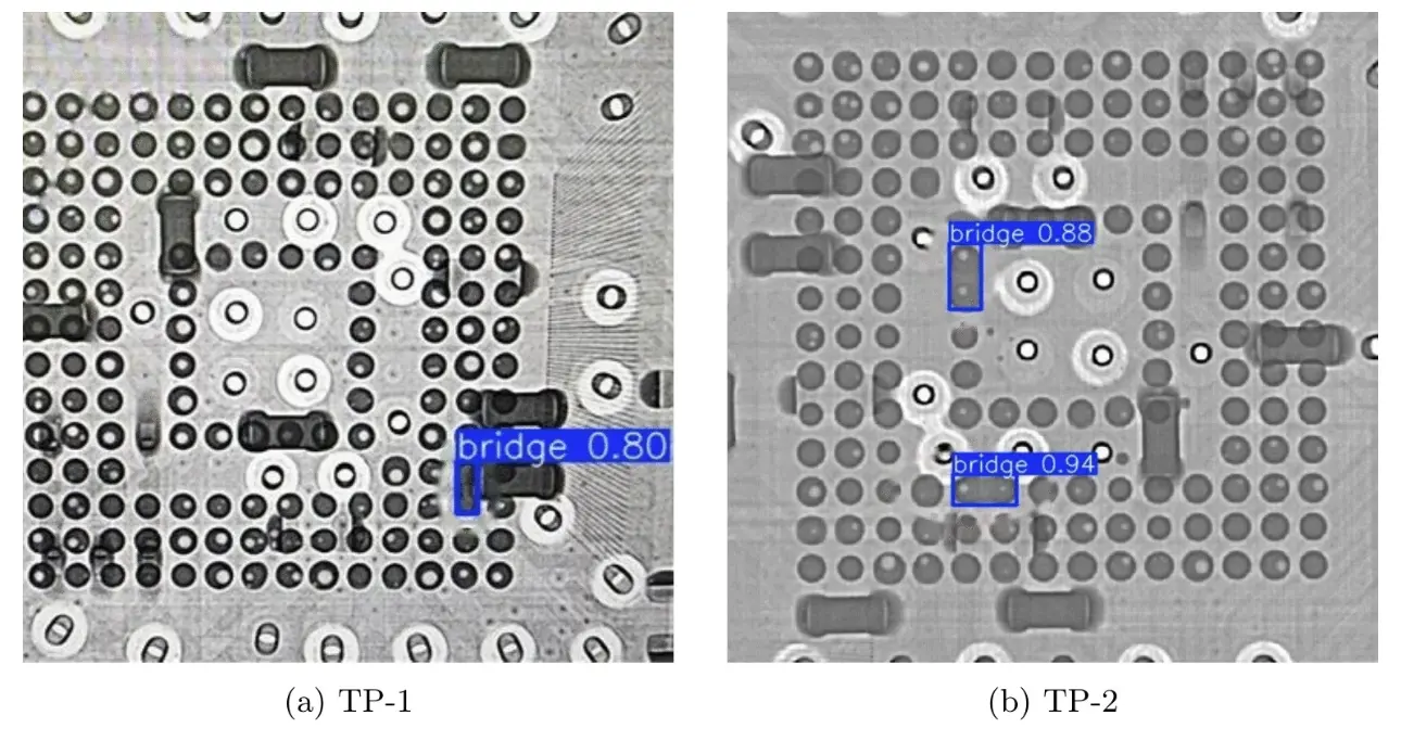
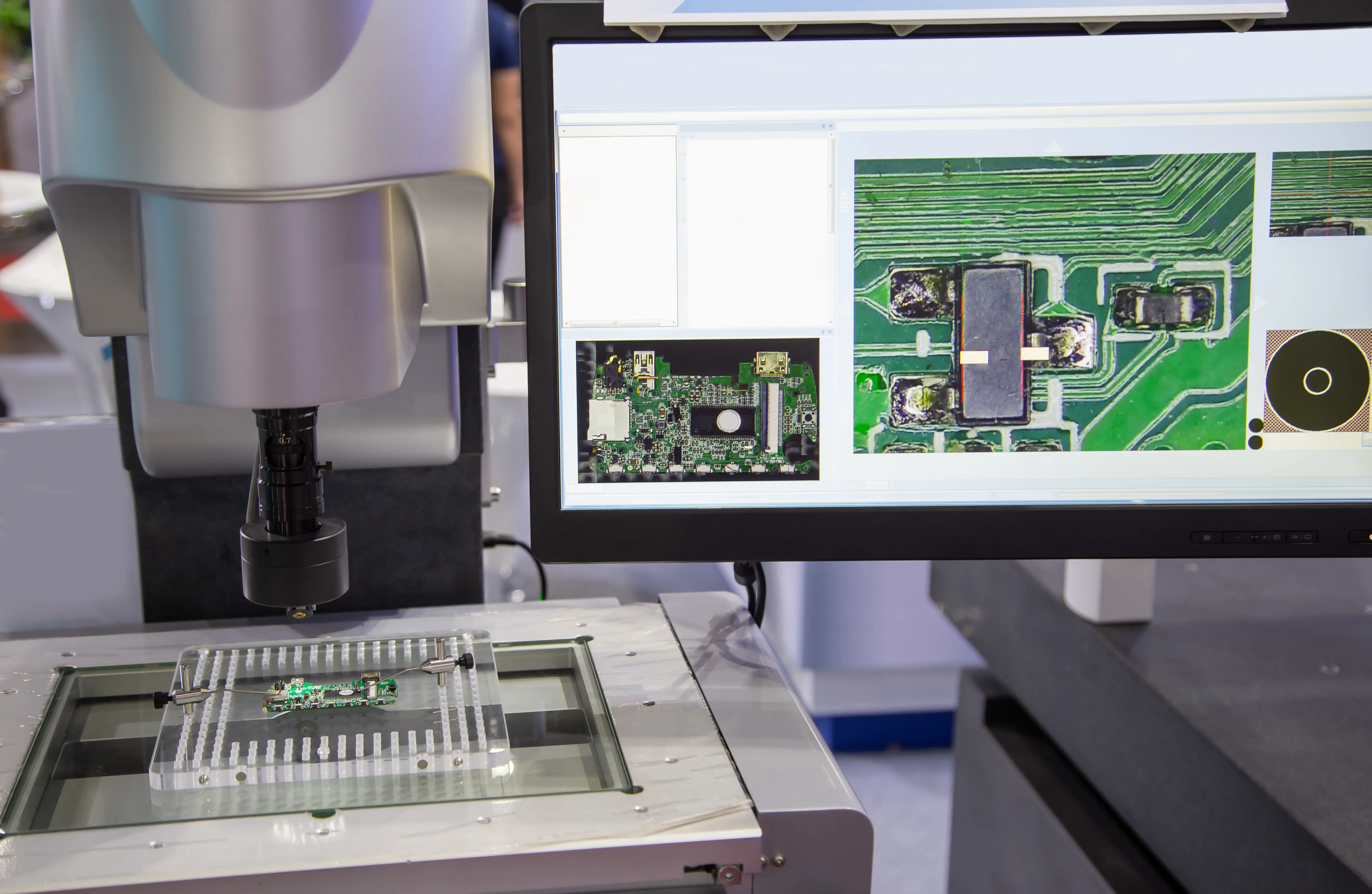
Manual inspection uses magnifiers or microscopes to examine solder fillets, component orientation and polarity while automated optical inspection (AOI) systems use high‑resolution cameras and image processing to compare each board against CAD data. AOI is useful for surface defects such as inadequate solder, open circuits, solder shorts and bridges.
When prototypes use ball‑grid arrays (BGAs) or other bottom‑terminated components, automated X‑ray inspection (AXI) is also used as it reveals volumetric defects, such as voids, bridging and internal misalignment that optical methods cannot see [1]. AOI and AXI systems in prototyping are often semi‑automatic rather than in‑line, but they provide invaluable feedback on design for manufacturability before high‑volume production.
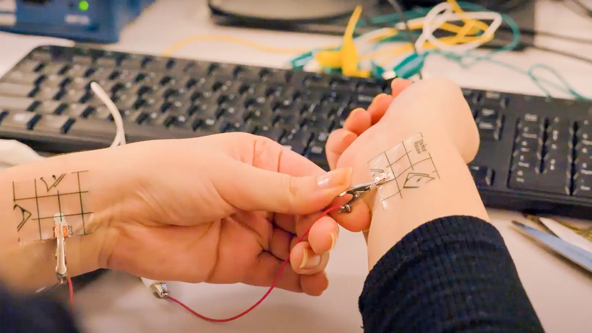
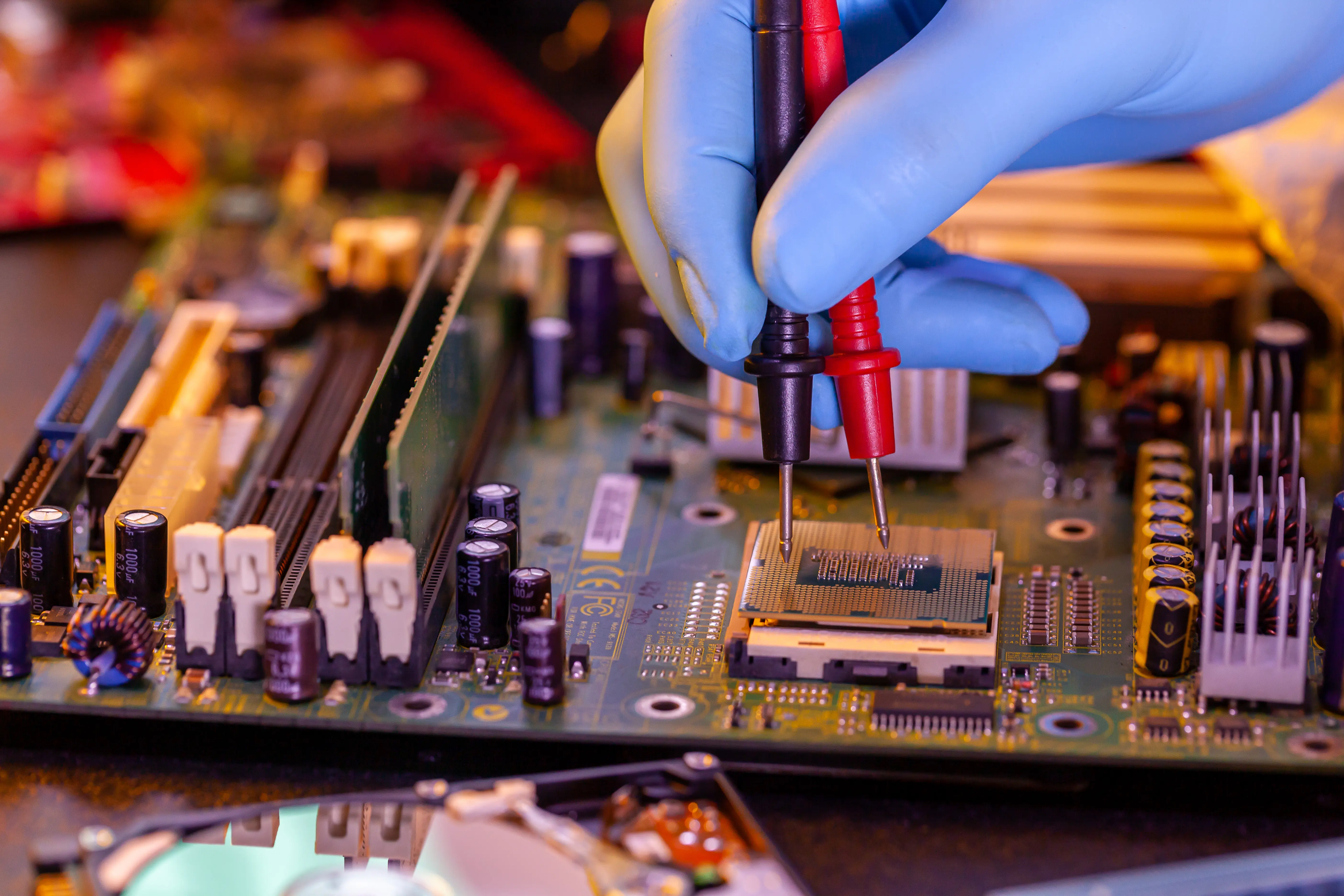
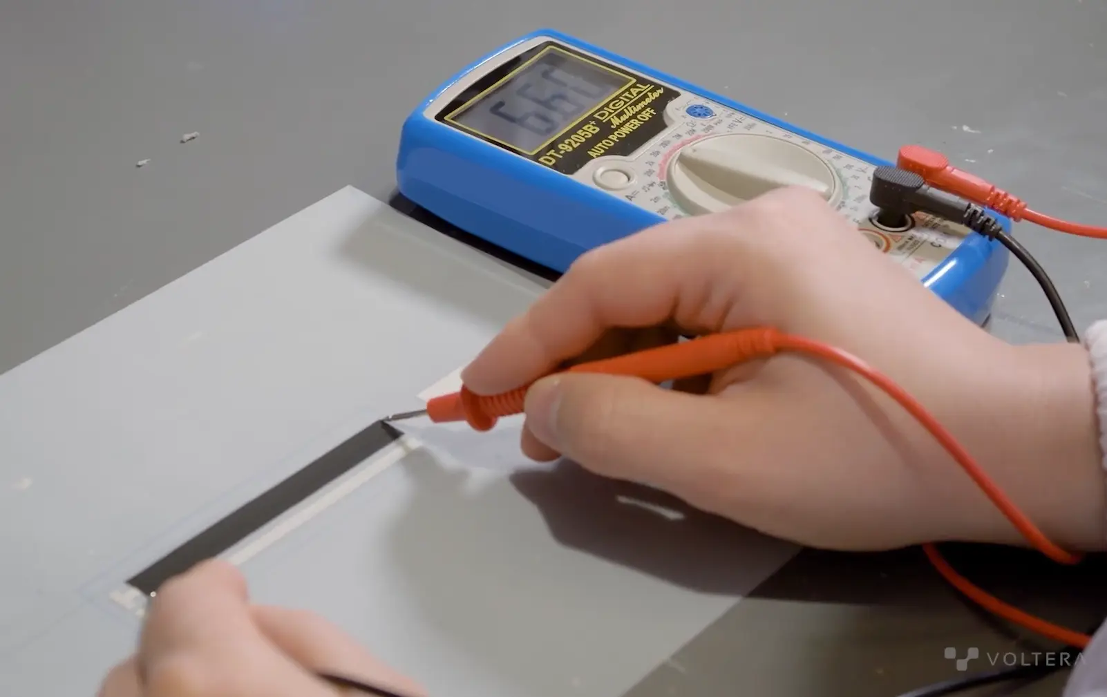
Electrical verification
This step is inexpensive and catches gross errors early. Prototype designs benefit from accessible test points or header connections to simplify probing. Engineers typically perform continuity and short checks with multimeters, measuring resistance, capacitance or diode drops at critical nodes to ensure that passive values are within tolerance.
Functional prototype tests
Functional tests at the prototype stage are typically bespoke and evolve with the design. They generate stimulus patterns and measure responses to emulate the normal operation of the circuit. The test system may be a bench setup using oscilloscopes, logic analyzers and programmable power supplies, or it can be a small fixture connecting to edge connectors or header pins. Firmware running on the board is often modified to support test hooks such as loopback modes or telemetry outputs. For analog or RF circuits, engineers measure frequency response, gain, or output power. For digital systems, they verify communication protocols and microcontroller functionality [2].
Types of PCBA tests in the manufacturing stage
Different from prototyping builds, production builds involve high volumes and strict quality control. The goal of testing at this stage shifts toward maximizing fault coverage, repeatability, and throughput, prioritizing automation and utilizing custom fixtures to prevent costly field failures.
AOI and AXI
At this stage, AOI and AXI complement each other to detect soldering defects and component misplacement quickly on every board. In-line AOI systems use cameras and machine‑vision algorithms to detect surface flaws such as insufficient or excess solder, tombstoning and misaligned parts while AXI provides radiographic images for packages like BGAs and quad‑flat no‑lead (QFN) to reveal voids, bridging, open circuits and internal misalignment and even inspect buried vias and multilayer connectivity [1].
Electrical connectivity tests
In these tests, in‑circuit testing (ICT) and flying probe are used to verify that there are no shorts or opens and that discrete components and networks meet tolerance before powering the assembly. ICT systems inject stimulus and measure voltages and currents to check component values, shorts and opens; they can achieve fault coverage above 90% when properly designed. Flying‑probe testers use a small number of movable probes that sequentially contact test points. They are slower than ICT but eliminate the need for custom fixtures, making them suitable for low‑volume or quick‑turn production.
System‑level testing
These functional tests help confirm that the assembled board operates according to specifications under real or simulated conditions. Similar to functional tests in the prototyping stage, these tests apply power and run firmware to exercise the board’s intended functions. Test fixtures may include power supplies, communication interfaces, loads and sensors.
Reliability and accelerated aging tests
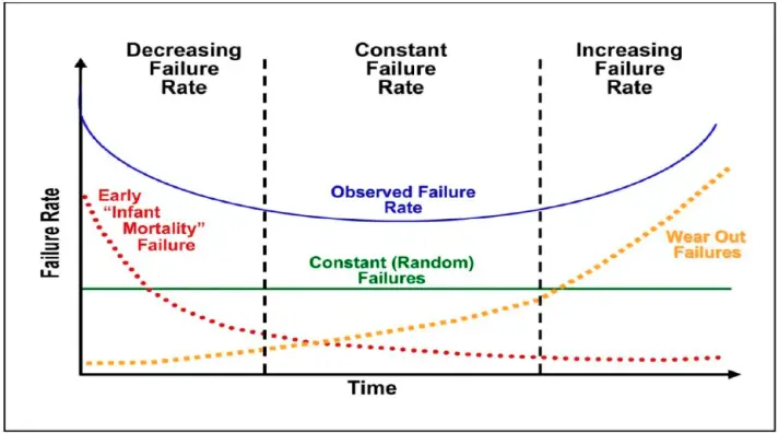
Reliability testing ensures that boards will remain fucntional over their service life by uncovering latent defects and wear‑out mechanisms. It is usually applied to sample units rather than every board. These tests subject assemblies to environmental stresses and monitor performance over time.
Burn‑in testing operates boards at elevated temperatures and voltages for extended periods to precipitate early failures. Highly accelerated life testing (HALT) and highly accelerated stress screening (HASS) cycle boards through extreme temperatures, humidity and vibration to identify weak points. Temperature‑humidity bias testing applies voltage while cycling environmental conditions to reveal corrosion or leakage. Reliability tests may also include vibration and shock testing, especially for automotive or aerospace products.
| Test type | Prototyping | Manufacturing |
|---|---|---|
| AOI/AXI | Minimal | Inline, strict pass/fail |
| Electrical connectivity | Multimeter | ICT/flying probe |
| Functional tests | Typically bespoke using desktop tools | Typically automated using dedicated test fixtures |
| Reliability tests | N/A | Sample-based (burn-in, HALT, HASS) |
Conclusion
Post‑assembly testing bridges the gap between theoretical design and real‑world performance. A holistic testing procedure provides full coverage from catching assembly errors, finding shorts and opens to predicting long‑term performance. By investing in the right tools for each stage, engineers can balance coverage, cost and speed in both prototyping and production, leading to higher‑quality products and fewer field failures.
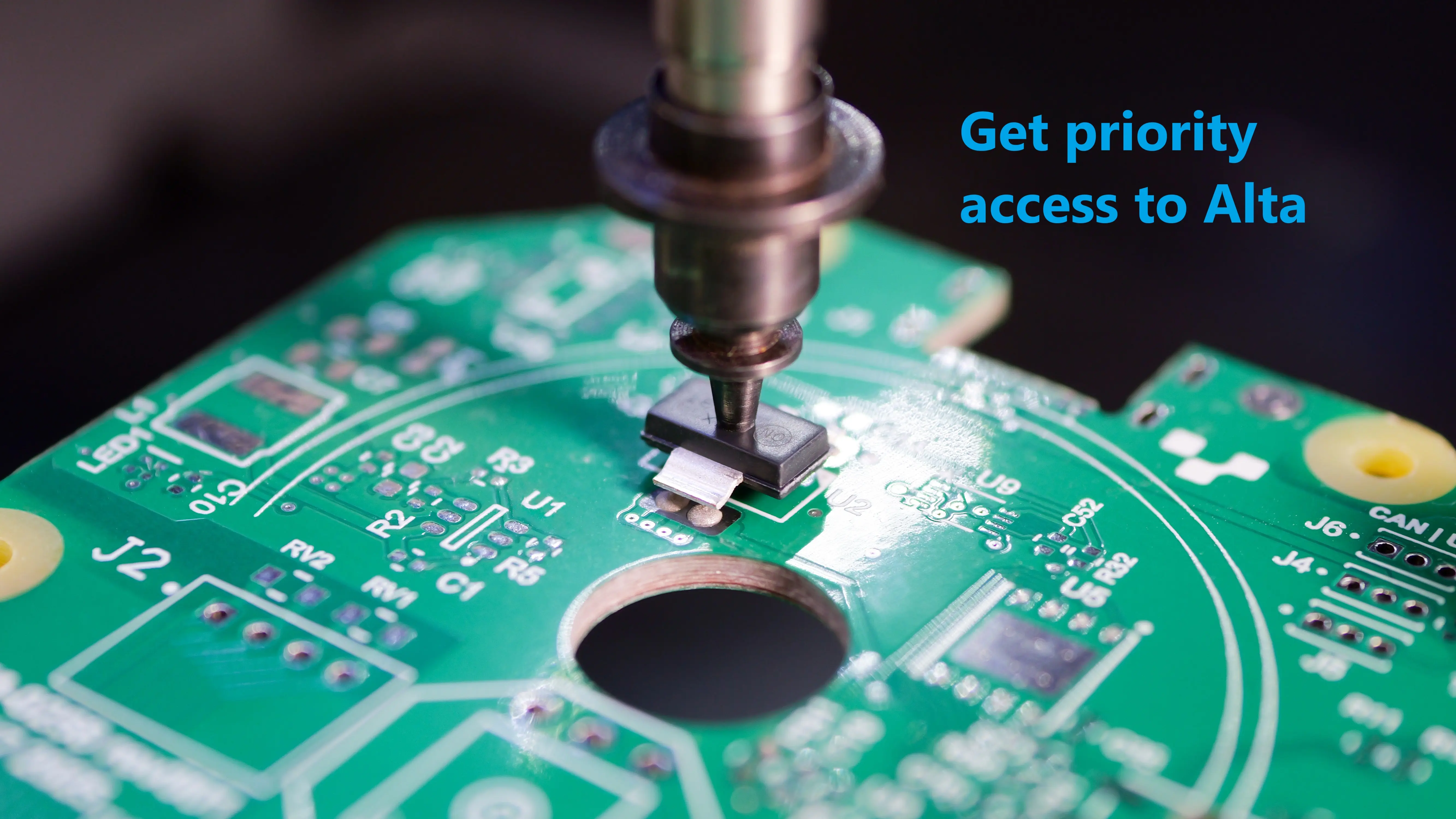
Looking for the right tool to test your PCBAs during prototyping? Don’t miss limited priority access to the Voltera Alta, a pick and place machine with smart AOI capability.
Want to learn more about choosing the right PCBA prototyping machine? Check out the following blogs:
References
[1] Roy, A., Hasan, A., Ghosh, S., Varshney, N., Julia, J., Reza Forghani, & Navid Asadizanjani. (2024). Applications and Challenges of AI in PCB X-ray Inspection: A Comprehensive Study. ACM Journal on Emerging Technologies in Computing Systems. https://doi.org/10.1145/3703457.
[2] Coombs, C., & Holden H. (2016). Printed Circuits Handbook, Seventh Edition. McGraw-Hill Education.
Check out our Customer Stories
Take a closer look at what our customers are doing in the industry.