PCBA Manufacturing Explained: Challenges and Opportunities
Printed circuit board assembly (PCBA) manufacturing is a core pillar of hardware development as it converts circuit designs into working products and connects every stage from pilot builds to mass production. For new product introduction (NPI), whether producing small pilot runs or scaling to volume, PCBA manufacturing directly affects product quality, reliability, cost, and ultimately the success of a product launch.
What is PCBA manufacturing
PCBA manufacturing is the controlled conversion of a PCB design into a repeatable, testable, shippable electronic subassembly by integrating materials (board and components), soldering processes (primarily surface mount technology/SMT). Inspection and testing gates then determine yield, reliability, compliance, and ramp speed [1].
Stages of PCBA manufacturing
| Step | Action | Description |
|---|---|---|
| 1 | Printed circuit board loading | Bare boards are fed into the assembly line. |
| 2 | Dust removal (cleaning) | Ensuring the surface is free of debris for better adhesion. |
| 3 | Solder paste printing | Applying solder paste on the boards through a stencil. |
| 4 | Solder paste inspection |
|
| 5 | Component placement | Setting up the pick and place machine, which then loads and mounts the surface mount device (SMD) components. |
| 6 | Pre-reflow inspection |
Inspections could include automated optical inspection (AOI) and others.
|
| 7 | Reflow soldering |
|
| 8 | Post-reflow inspection |
Inspections could include automated X-ray inspection (AXI), in-circuit test (ICT), and AOI.
|
| 9 | QC confirmation |
|
| 10 | Transfer to dual in-line package (DIP) | Move the board to the through-hole stage. |
Adapted from “SMT production process” © Lu, S., et., al
Industry trends in PCBA manufacturing
According to research and market’s 2026 report, the SMT market is projected to expand significantly, reaching approximately $9.56 billion USD by 2030 at a compound annual growth rate of 9.5%. Key shifts shaping PCBA manufacturing include component miniaturization, increased reliance on automated inspection, and supply-chain volatility.
Component miniaturization
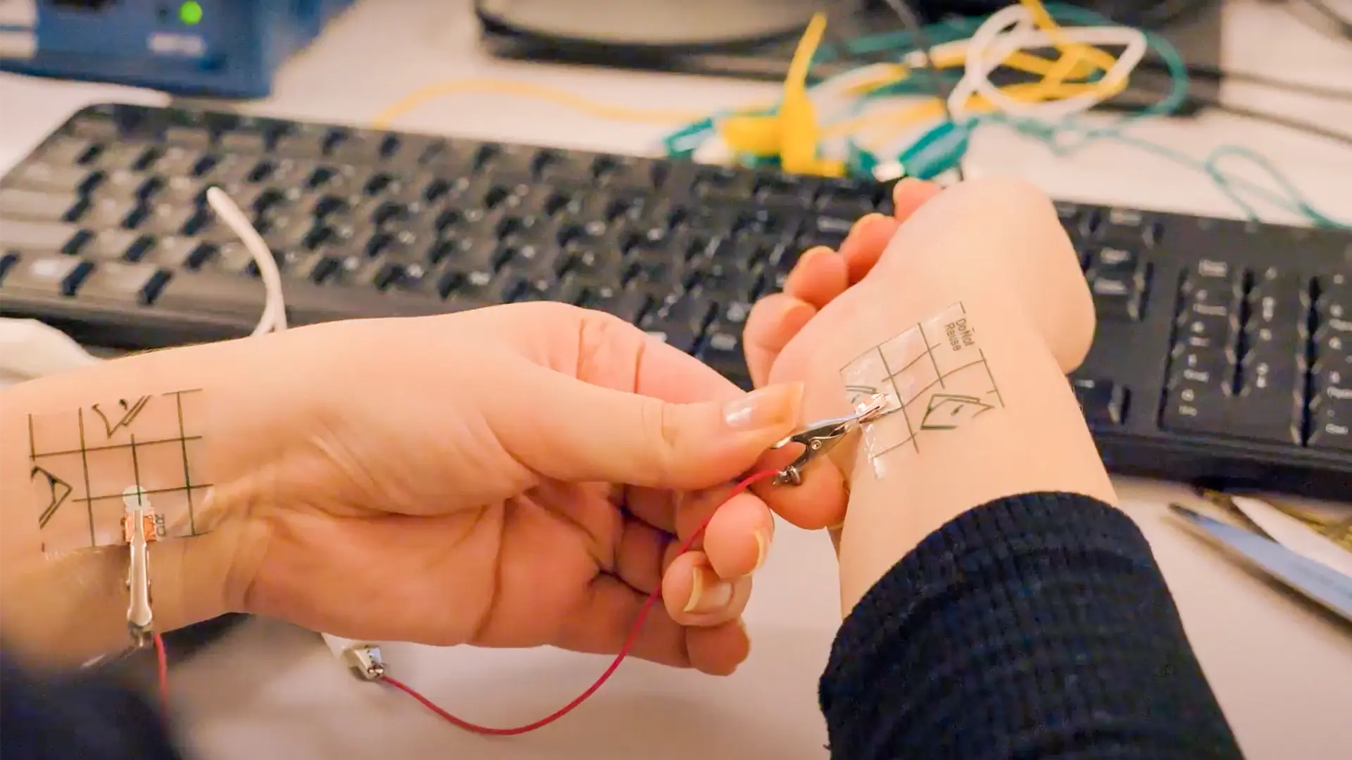
As wearables, consumer electronics, and medical devices become more lightweight and compact, they require smaller components and more integrated designs, which directly drives smaller SMD packages and higher density layouts. From fine-pitch quad-flat no-leads (QFN) to solderless micro ball grid arrays (BGA), these components create reliability risks such as electromigration and thermomigration [2].
This doesn’t mean, however, that the companies that shrink fastest will be the ones that succeed. Instead, companies that succeed are the ones that manage risk holistically through design for manufacturability, materials reliability strategies, and robust inspection and testing programs [3].
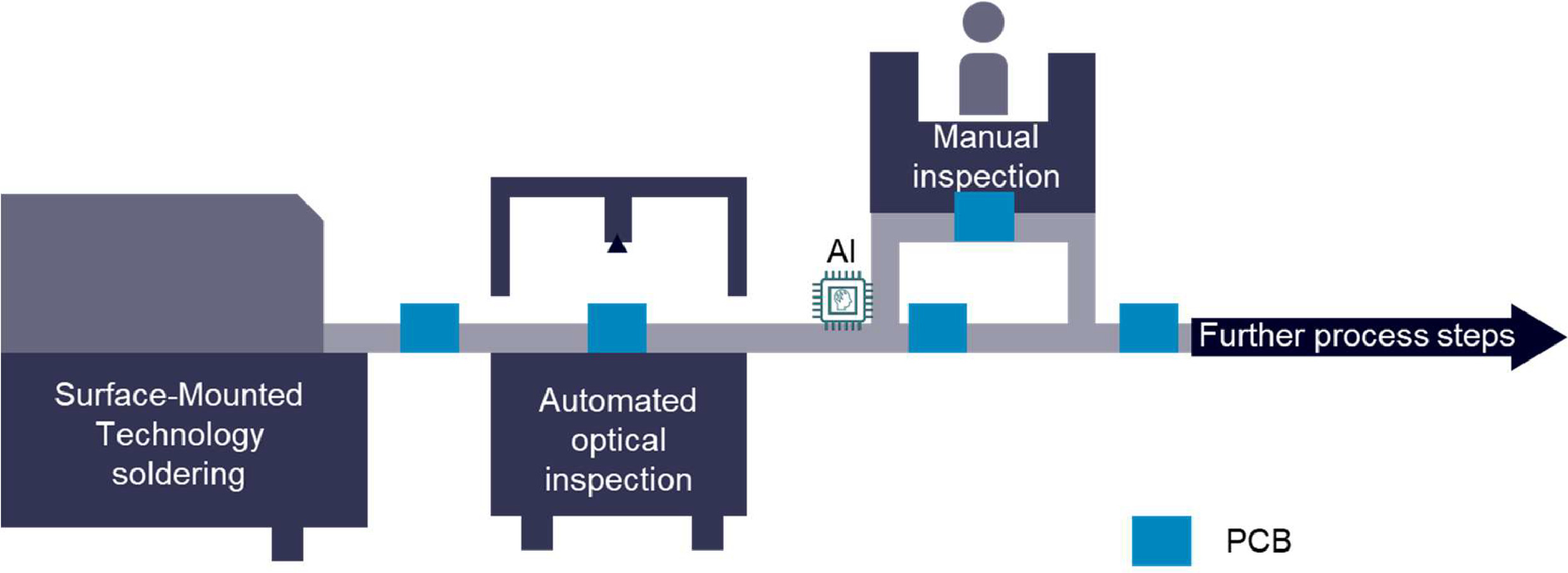
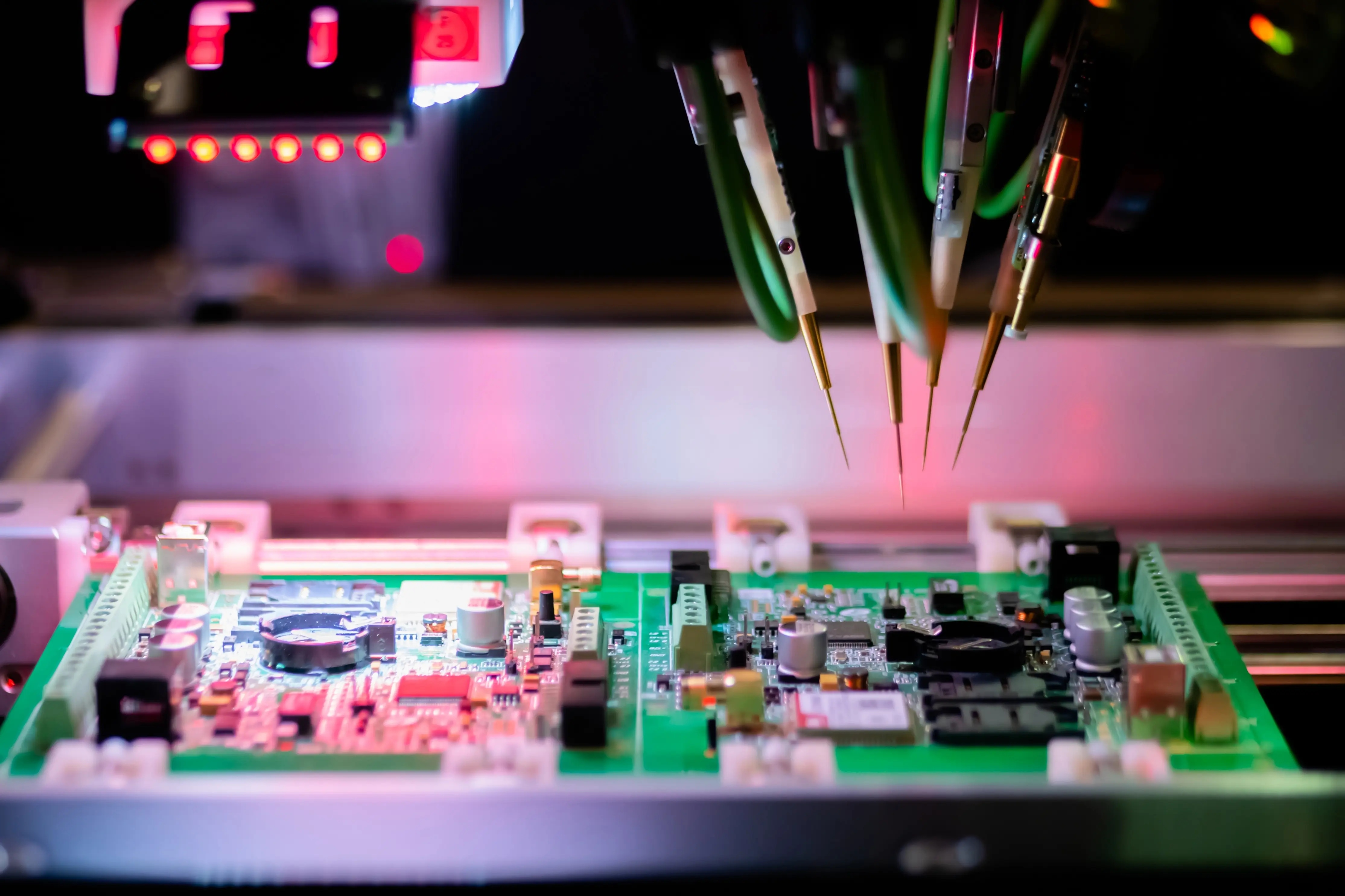
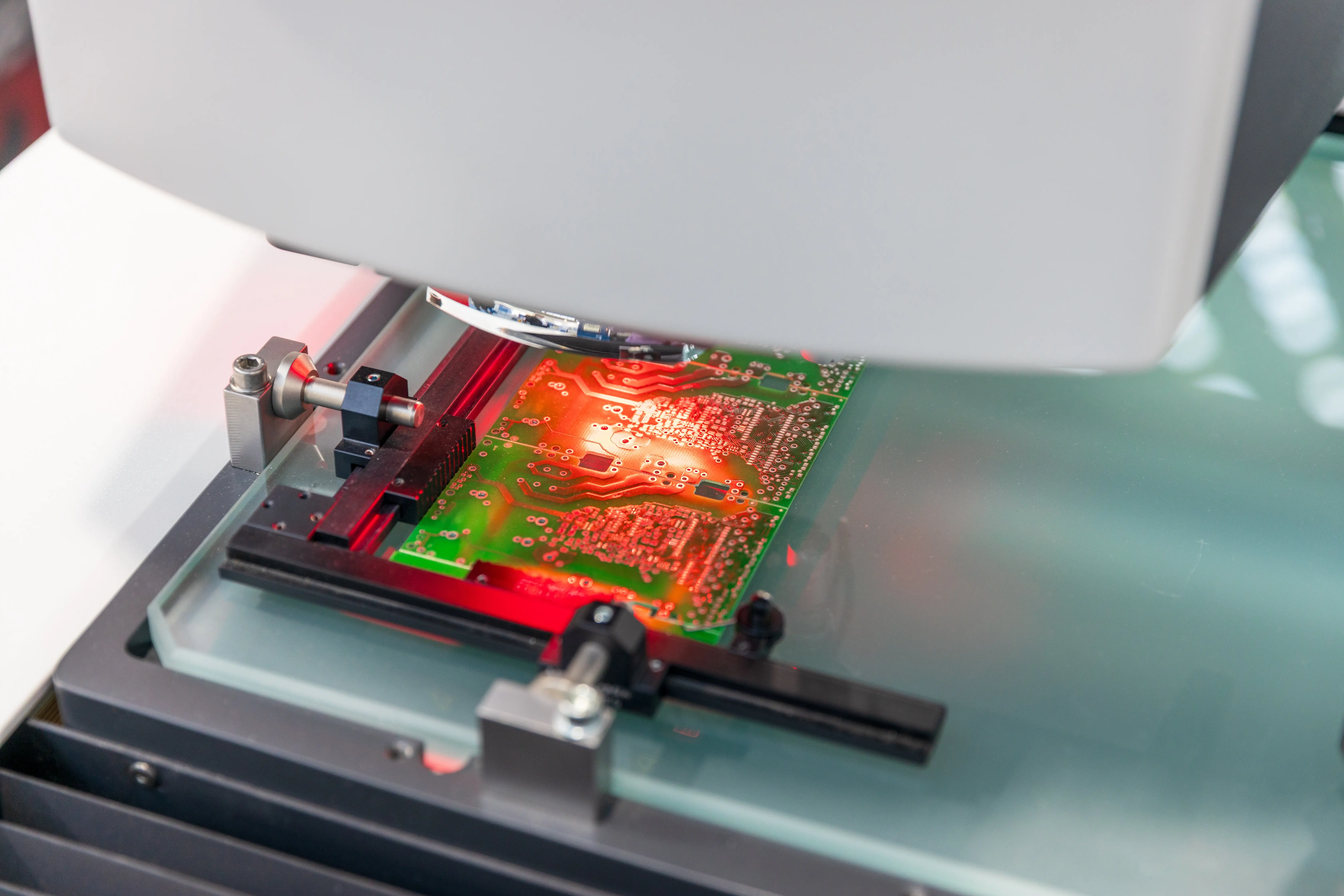
Machine and deep learning for automated optical inspection
Automated optical inspection (AOI) is now standard across SMT production, yet its effectiveness is constrained by false calls that require manual review. One study [4] found that among AOI-flagged samples routed to manual inspection, false calls vastly outnumbered real defects (435,652 false calls vs. 4,622 true defects over 132 days). This demonstrates how AOI thresholding and decision logic can become a throughput constraint in practice.
Deep learning-based inspection systems are emerging to address this imbalance. Recent work demonstrates that AI-driven solder-joint detection can significantly reduce false positives and improve consistency in identifying subtle defects, enabling inspection to shift from rule-based filtering toward data-driven decision support [5].
Supply chain risks
The SMD components supply chain is vulnerable to disruptions from geopolitics, natural disasters, IP risks, and demand spikes. For example, the median inventory for key semiconductors in the US fell from 40 days (2019) to 5 days (2021) while median demand was 17% higher. Chip shortages during the COVID-19 pandemic was estimated to have cost the global economy $240 billion.The supply chain vulnerability continued in the post-pandemic era, with components like memory chips still facing significant shortage, stretching into 2027.
In response, governments and industry have accelerated reshoring efforts. In the U.S., for example, the CHIPS and Science Act represents a major policy push to expand domestic semiconductor manufacturing capacity and reduce reliance on overseas fabrication. While there have been lots of talks of reshoring, full localization is constrained by major barriers, such as high capital requirements, limited technical capacity, and long timelines to build fabrication infrastructure [6]. In practice, “regionalization” can be more realistic than full reshoring in high-specialization ecosystems, even after disruption events [7]. This means designing manufacturing packages (BOM alternates, process windows, inspection recipes) to be portable across regions and contract manufacturers, rather than deeply coupling to a single site’s tacit knowledge.
Conclusion
PCBA manufacturing sits at the intersection of design, materials, process engineering, and supply-chain strategy. As electronics become more compact and complex, success depends on process control, inspection maturity, and resilient sourcing strategies. Teams that embed manufacturability and inspection early in NPI with reliable pick and place and solder paste dispensing solutions are better positioned to scale from pilot builds to volume production while maintaining yield, reliability, and schedule certainty.
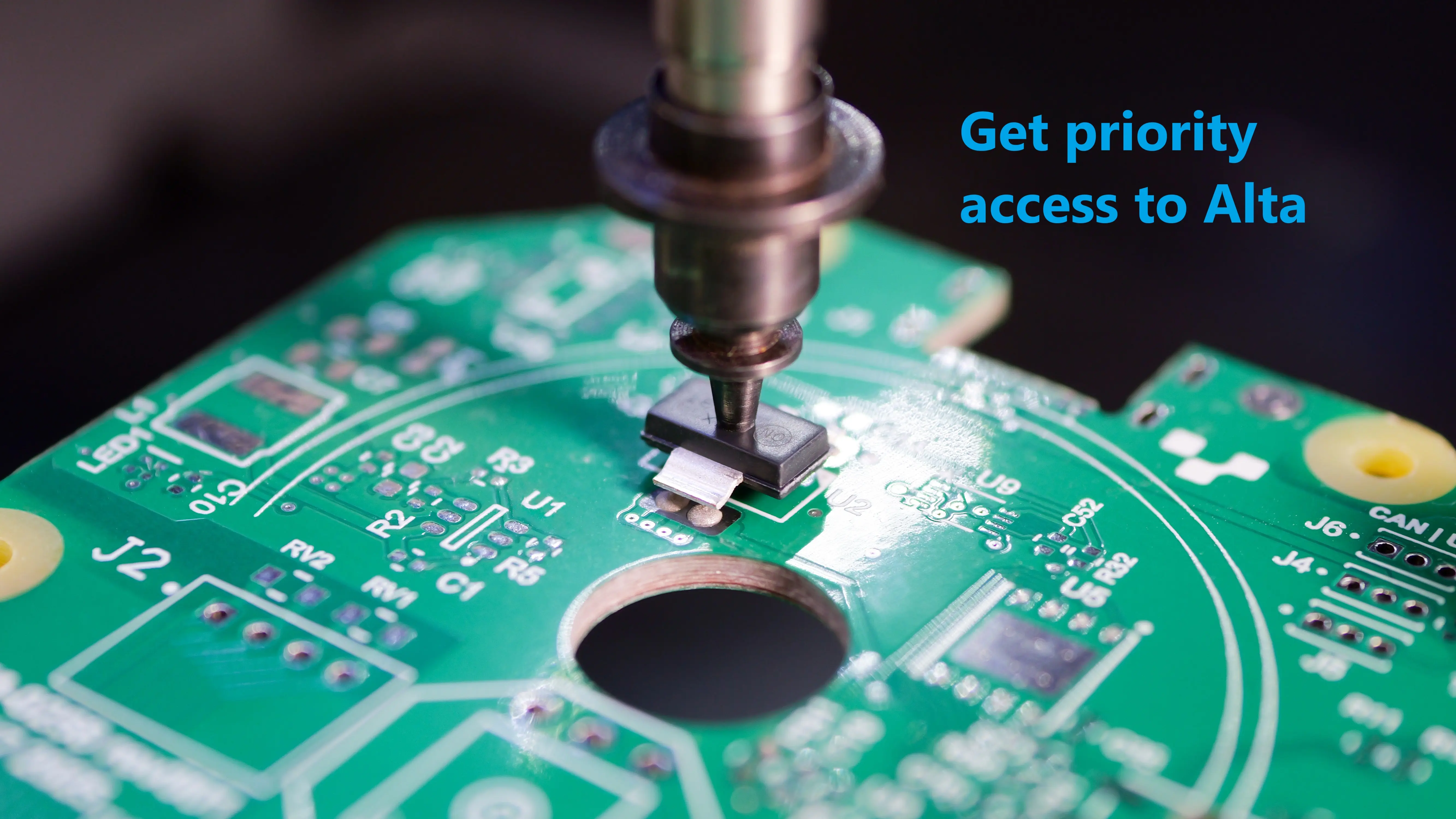
Looking for a pick and place machine built for prototyping? Don’t miss limited priority access to the Voltera Alta, a pick and place machine integrated with solder paste dispensing to make PCB assembly fast, easy, and enjoyable.
Want to learn more about PCBA manufacturing? Check out the following blogs:
References
[1] Petkov, N., & Ivanova, M. (2024). Printed circuit board and printed circuit board assembly methods for testing and visual inspection: a review. Bulletin of Electrical Engineering and Informatics, 13(4), 2566–2585. https://doi.org/10.11591/eei.v13i4.7601.
[2] Zhang, P., Xue, S., & Wang, J. (2020). New challenges of miniaturization of electronic devices: Electromigration and thermomigration in lead-free solder joints. Materials & Design, 192, 108726. https://doi.org/10.1016/j.matdes.2020.108726.
[3] Bender, E., Bernstein, J. B., & Boning, D. S. (2024). Modern Trends in Microelectronics Packaging Reliability Testing. Micromachines, 15(3), 398–398. https://doi.org/10.3390/mi15030398.
[4] Pfab, K., Eichler, R., Mallandur, A., & Rothering, M. (2024). Data of automated optical inspection of surface-mounted technology electronic production. Data in Brief, 53, 110110. https://doi.org/10.1016/j.dib.2024.110110.
[5] Iñigo Mendizabal-Arrieta, Álvarez, H., Aguinaga, D., Pellicer, A., Sánchez, J. R., & Torres, F. (2025). Deep learning-based solder joint defect detector. The International Journal of Advanced Manufacturing Technology. https://doi.org/10.1007/s00170-025-15460-8.
[6] Sergiu Metgher. (2025). Strategic Resilience and Reshoring: Reconfiguring Semiconductor Supply Chains in an Era of Global Disruptions. Emerging Frontiers Library for the American Journal of Engineering and Technology, 7(11), 232–238. https://emergingsociety.org/index.php/efltajet/article/view/577.
[7] Kamakura, N. (2022). From globalising to regionalising to reshoring value chains? The case of Japan’s semiconductor industry. Cambridge Journal of Regions, Economy and Society, 15(2). https://doi.org/10.1093/cjres/rsac010.

Check out our Customer Stories
Take a closer look at what our customers are doing in the industry.