Common Solder Paste Defects in PCBA Prototyping
Common Solder Paste Defects in PCBA Prototyping
- By: Shuxuan Jiang
- Published: July 31, 2026 |
Modified: August 5, 2026 - Estimated read time: 6 minutes
- By: Shuxuan Jiang
- Published: July 31, 2026 |
Modified: August 5, 2026 - Estimated read time: 6 minutes
- 1. Types of solder paste defects in PCB prototyping
- 2. Insufficient solder paste and missing deposits
- 3. Excessive solder paste and bridging
- 4. Solder offset and registration errors
- 5. Slump, spatter, and deposit shape instability
- 6. Voiding and other latent defects that begin at paste deposition
- 7. Conclusion
- 8. References
- 1. Types of solder paste defects in PCB prototyping
- 2. Insufficient solder paste and missing deposits
- 3. Excessive solder paste and bridging
- 4. Solder offset and registration errors
- 5. Slump, spatter, and deposit shape instability
- 6. Voiding and other latent defects that begin at paste deposition
- 7. Conclusion
- 8. References
Solder paste deposition happens at the start of surface mount technology (SMT) assembly, but problems introduced at this stage often don’t show up until much later, and can carry through to component placement and reflow. In PCBA manufacturing, that makes solder paste defects especially costly: more than 50% of SMT defects have been traced back to the solder paste deposition stage [1]. By the time a defect becomes visible, the board may have already moved through several process steps, driving up the cost of inspection, rework, and lost production time.
The stakes look different in PCB assembly prototyping, but the disruption is just as real. A defective deposit might affect only one board instead of an entire production run, but a build intended to deliver quick design feedback can turn into hours of troubleshooting and manual rework. In some cases, it can consume more engineering time than assembling another revision from scratch.
For prototyping teams, knowing how solder paste defects originate, and how to catch them before they become solder joint failures, protects both assembly quality and iteration speed.
Types of solder paste defects in PCB prototyping
Research on solder paste printing inspection identifies six common visible post-deposition defects: excessive solder, insufficient solder, solder offset, solder bridging, missing deposits, and solder spatter [2].
Insufficient solder paste and missing deposits
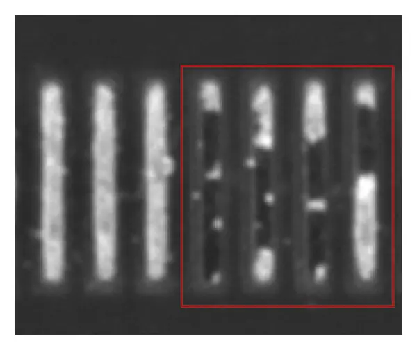
Insufficient solder paste occurs when a pad receives too little paste, or none at all, leaving the resulting joint with poor wetting, weak mechanical support, or an open connection after reflow. In prototyping, it often shows up as a single component on an otherwise clean board that fails electrical testing while everything around it passes.
The causes are rarely random. When using stencils, solder paste deposition depends on aperture size, printing speed, and paste particle size — three factors that determine how much solder paste actually transfers from the stencil onto the PCB pads. In other words, insufficient solder paste is often caused by too little solder paste being deposited on the pad, long before it becomes a soldering problem [3].
Excessive solder paste and bridging
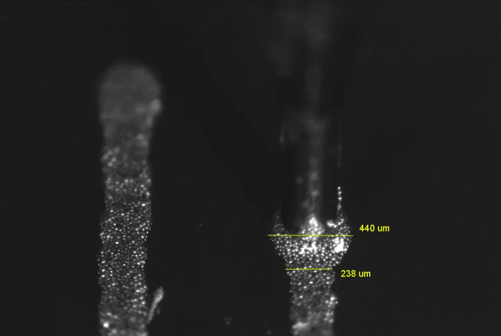
When deposits are too large for the pad geometry, the risk of poor standoff, solder balls, and solder bridging between adjacent pads goes up.
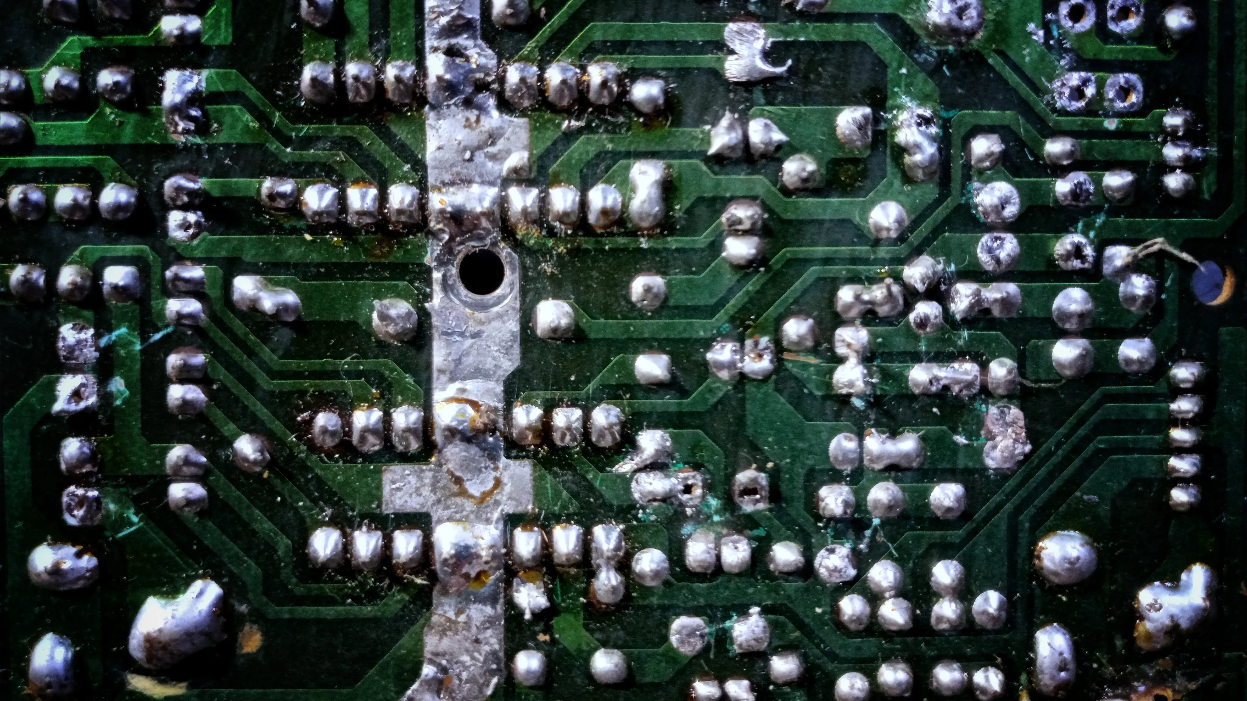
Bridging isn't only a volume problem; it's also a function of paste rheology, flux chemistry, and how the paste behaves over time. For example, a study on type 7 solder paste for fine-pitch interconnects found that at a 0.08 mm pitch, two formulations containing both sebacic and suberic acid showed no slumping or bridging, while a third formulation containing only suberic acid showed dewetting and bridging at the same pitch [4].
Solder offset and registration errors
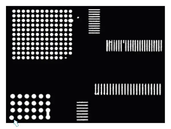
Offset defects happen when paste lands in the wrong place relative to the pad. Even when deposit volume is correct, the paste is already misaligned before a component is ever placed. In prototyping, this often traces back to imperfect board alignment, issues translating CAD data into machine coordinates, or small setup inconsistencies between boards.
Solder paste offset and volume both influence how much a component shifts on the wet paste during placement. If the paste is off-center, the component begins placement from an incorrect position, and self-alignment during reflow won't always correct for it [5].
Slump, spatter, and deposit shape instability
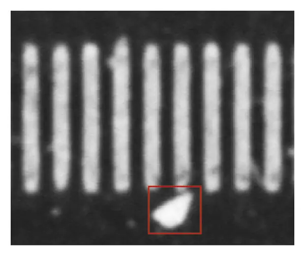
Some solder paste defects are shape problems rather than volume or placement problems. Paste can spread after deposition, split into irregular shapes, or leave small spattered deposits outside the intended pad area. These defects often appear intermittently: The first board may look fine, the third may show inconsistent deposits, and the fifth suddenly shows bridging.
Like volume problems, shape instability often points back to paste formulation. There is a real trade-off between printability, wettability, and viscosity stability over time [4]. Process physics plays a role too: changes in paste chemistry and particle-surface condition can cause coarsening, viscosity instability, and poor deposition behavior overall.
Voiding and other latent defects that begin at paste deposition
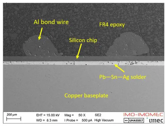
Voiding often isn't visible until after reflow or X-ray inspection, but it's more than a downstream soldering problem; the deposition workflow plays a meaningful role in how voids form in the first place.
One study found that more aggressive flux reduced void area, with one paste showing roughly 20% lower void content than another, and that modified stencil apertures produced substantially lower void formation than standard designs [6]. Another study similarly found that greater solder paste volume was associated with larger voids in SAC-based solder joints [7]. For prototyping teams, that means voiding can start with how much paste was deposited, where it was deposited, and how easily volatiles can escape during heating.
Conclusion
Insufficient paste, excess paste, offset, bridging, missing deposits, slump, spatter, and voiding all trace back to the same underlying question: how well does your process control deposit geometry and location on the board you're building today?
Recognizing which defect you're looking at and why it happened is the first step. Stay tuned for our upcoming blog post which explains how to troubleshoot and resolve each of these defects during prototyping.
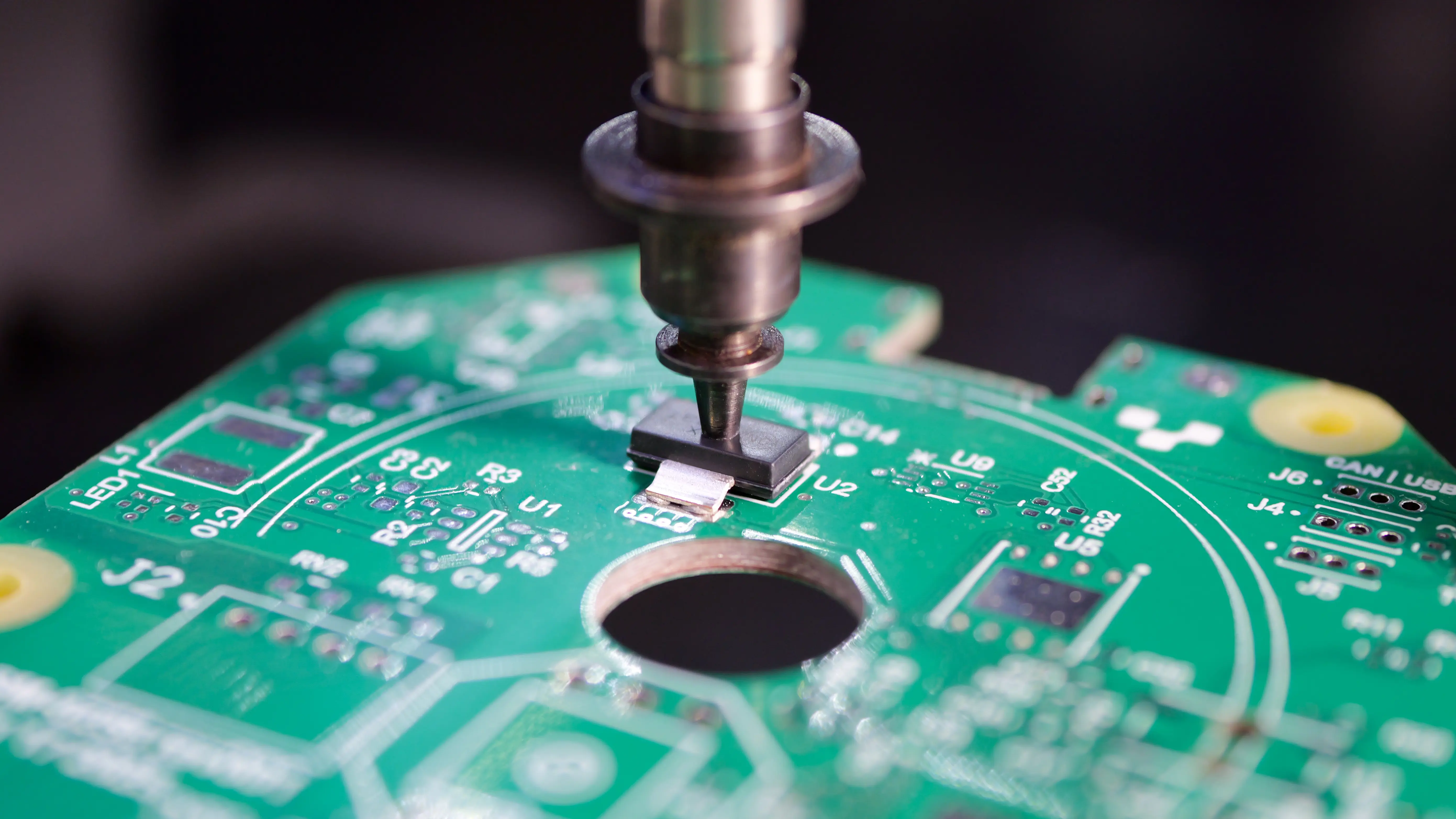
Did you know Voltera has a new product? It’s a pick and place machine with stencil-free solder dispensing, guided setup, machine vision, and accessible inspection. It makes PCB assembly faster while making solder paste defects easier to catch before they turn into rework. Interested in learning more? Sign up to get Alta updates.
Want to learn more about prototyping PCB assembly? Check out these blogs:
References
[1] Cao, N., Farrag, A., Won, D., & Yoon, S. W. (2024). XSCAN: Explainable solder joint defect probability prediction through solder paste printing status with imbalanced data. Journal of Manufacturing Systems, 77, 212–227. https://doi.org/10.1016/j.jmsy.2024.09.009.
[2] Qi, M., Yin, T., Cheng, G., Xu, Y., Meng, H., Wang, Y., & Cui, S. (2022). Research on Printing Defects Inspection of Solder Paste Images. Wireless Communications and Mobile Computing, 2022(1). https://doi.org/10.1155/2022/8651956.
[3] Martinek P, Illés B, Codreanu N, Krammer O. Investigating Machine Learning Techniques for Predicting the Process Characteristics of Stencil Printing. Materials. 2022; 15(14):4734. https://doi.org/10.3390/ma15144734.
[4] Choi, Dong–Gyu & Park, Si & Mhin, Sungwook & Hong, Won Sik & Yoo, Sehoon. (2024). Printability Evaluation of Water-Soluble Type 7 Solder Paste for Fine Pitch Advanced Package Interconnects. 2024 IEEE 26th Electronics Packaging Technology Conference (EPTC). 774-777. 10.1109/EPTC62800.2024.10909844.
[5] Cao, S., Parviziomran, I., Yang, H., Park, S., & Won, D. (2019). Prediction of Component Shifts in Pick and Place Process of Surface Mount Technology Using Support Vector Regression. Procedia Manufacturing, 39, 210–217. https://doi.org/10.1016/j.promfg.2020.01.316.
[6] Kozak, M., Vesely, P., & Dusek, K. (2023). Analysis of solder mask roughness and stencil shape influence on void formation in solder joints. Welding in the World, 67(5), 1347–1355. https://doi.org/10.1007/s40194-023-01505-7
[7] Alakayleh, A., Hamasha, S., & Alahmer, A. (2024). The impact of paste alloy, paste volume, and surface finish on solder joint. Microelectronics Reliability, 160, 115457. https://doi.org/10.1016/j.microrel.2024.115457.
Check out our customer stories
Take a closer look at what our customers are doing in the industry.