Overcoming Challenges of PCBA Prototyping
Picture this: you're a hardware engineer in R&D at an electronics development company. You’re in rapid-iteration mode: a new board revision came back, the schematic “looks right,” and the team needs proof by noon that the power path is stable and the main control unit boots reliably.
A day in the life of a hardware engineer
In the morning, your plan is simple: assemble a small set of boards, run bring-up scripts, and walk into a 4 p.m. demo with clean data.
Instead, the first hours disappear into setup work: sourcing replacement components, reconciling reels with BOM entries, and configuring a pick and place machine designed more for production runs than quick iteration.
By noon, one board partially powers on, but several questions remain. Is the short caused by a solder paste bridge, a rotated component, or a footprint mismatch?
At 4 p.m., the team reviews results from a board that passes only part of the test sequence. Another revision is scheduled, because isolating the root cause through manual debugging takes longer than rebuilding the board.
The next day looks familiar: instead of iterating on the design, much of the effort goes into managing assembly steps, troubleshooting setups, and repeating work that should be consistent from build to build.
The pain of prototyping PCBAs, in real practitioners’ words
That stagnation is the signature failure mode of PCBA prototyping without tools and workflows built for iteration. As a hardware engineer recently told us,
“By the time we kit up parts for ten boards, ship them to China, have them assembled, and then shipped back to us, it’s six to eight weeks. Because of that, we typically try to do hand assembly on prototype boards as we do new designs. But it’s mind-numbing, repetitive under a microscope, picking up 0402s with tweezers.”—Hardware team lead, Canadian technology company
Why PCBA prototyping is uniquely difficult
PCBA prototyping amplifies small, ordinary sources of variation because there’s little statistical cushioning and almost no slack time.
Smaller batches are less forgiving
If you build 5 to 20 boards, a single recurring defect mode, for example insufficient solder on one pad geometry, can wipe out most of the batch. In contrast to production, you can’t always average out process drift with large numbers. Every board represents a larger fraction of your learning budget.
High revision frequency
Compared to breadboards, PCBA prototypes are harder to modify, are often one-off, and routinely trigger rebuilds rather than clean disassembly and reuse. This is partly because soldering and desoldering are tedious and failure-prone at small geometries.
Low margin of error for small passives
In general, smaller components can exhibit more severe misalignment under identical printing and placement conditions. For small passives, misalignment and reflow dynamics can produce defects like tombstoning, where one end lifts due to unequal wetting forces during reflow.
Tools not built for high-mix environments
Production SMT tools can be extremely capable in terms of throughput, but they’re optimized for the wrong objective function when the goal is rapid iteration and learning. High-mix environments are known to be changeover-driven, and without proper pick and place solutions that are prototyping-friendly, the process can become riddled with downtime.
Common points of failure in PCBA prototyping
The failure modes of prototyping are not mysterious; they cluster at predictable interfaces between design elements, material handling, operator training, and equipment [1].
| Stage | Typical prototyping failures |
|---|---|
| Design |
|
| Soldering |
|
| Component placement |
|
| Reflow |
|
| Inspection |
|
| Process bottlenecks |
|
Overcoming the challenges in PCBA prototyping
A useful mental model is to treat prototyping as a closed-loop control problem: reduce variance, tighten feedback, and make the loop affordable enough to run often.
Design right
A practical baseline of DFM is to align land patterns and clearances with IPC guidance (IPC-7351), which explicitly covers land pattern geometries and recommendations for adjacent component clearances and related design elements. For hardware engineers, the actionable shift is to treat libraries as controlled assets: version them, approve them, and capture deviations from standards as explicit, reviewable engineering decisions.
Assemble right
Solder paste issues account for a large portion of defects (about 52%-71%), and rework and repeated reflow cycles can change solder joint microstructure and compromise strength by up to 20%-35%. It’s therefore important to have an assembly workflow that minimizes variability in the solder paste dispensing, component placement, and reflow process — a prototyping-friendly PCB assembly solution such as Alta.
This means adopting pick and place machines built for agile prototyping, with smart feeders and part handling where possible, automated alignment and solder paste dispensing, and built-in settings that “just work” for repeat builds. This reduces manual handling and associated uncontrolled error, as well as changeovers, downtime, missed deadlines, and escalating costs in prototyping environments [2].
Validate right
Even with the right tools, defects and design issues are inevitable. What matters is how quickly they are detected and diagnosed. Without a structured inspection and validation strategy, teams often discover problems late in the process, such as during firmware bring-up or system integration, when the root cause becomes harder to isolate.
A practical validation workflow introduces graduated inspection and testing steps before full functional evaluation. Initial inspection should verify assembly integrity through visual inspection or automated optical inspection (AOI). Once assembly quality is confirmed, boards should move through controlled electrical validation. Establishing this progression reduces the risk of damaging components during first power-up and helps isolate failures more efficiently. Finally, validation results should be documented alongside assembly parameters and design revisions for reference, accelerating subsequent prototype iterations.
Accelerating PCBA prototyping
With the right processes and tools, prototyping PCBAs should no longer be an ordeal, and hardware engineers certainly don’t have to be disgruntled. If you’d like to measure how your pick and place process is slowing you down, take a look at our blog: Is Your Pick and Place Machine Helping or Holding You Back. If you’re looking to get an idea of what an agile process looks like, check out Why In-House PCB Assembly is the Next Leap for Agile Hardware Teams.
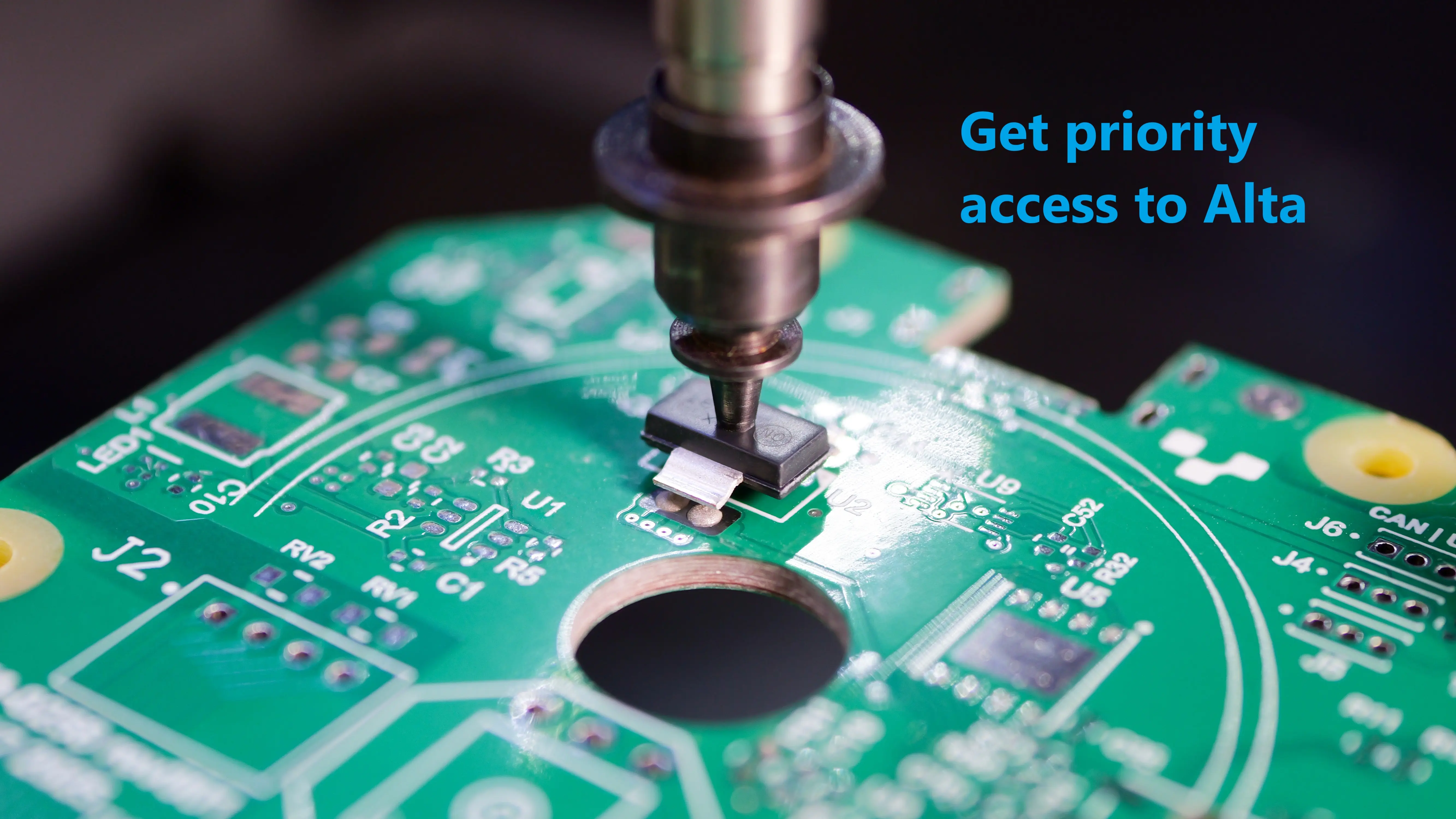
Looking for a pick and place machine built for prototyping? Don’t miss limited priority access to the Voltera Alta, a pick and place machine integrated with solder paste dispensing to make PCB assembly fast, easy, and enjoyable.
References
[1] Coombs, C., & Holden H. (2016). Printed Circuits Handbook, Seventh Edition. McGraw-Hill Education.
[2] Quijano, J., Torres Cruz, N., Quijano-Quian, L., Poblano-Ojinaga, E. R., & Noriega Morales, S. A. (2025). Data-Driven Scheduling Optimization for SMT Lines Using SMD Reel Commonality. Data, 10(2), 16. https://doi.org/10.3390/data10020016.
Check out our Customer Stories
Take a closer look at what our customers are doing in the industry.