From Vinyl Record Waste to PCBs With Voltera V-One
From Vinyl Record Waste to PCBs With Voltera V-One
- By: The Voltera Team
- Published: October 23, 2026 |
Modified: October 23, 2026 - Estimated read time: 7 minutes
- By: The Voltera Team
- Published: October 23, 2026 |
Modified: October 23, 2026 - Estimated read time: 7 minutes
- 1. The problem with a conventional PCB
- 2. Turning vinyl record waste into PCB substrates
- 3. Testing conductive materials with V-One
- 4. From prototyping to pilot production
- 5. Putting the process to the test: an FM radio, 84 years later
- 6. The environmental case
- 7. What comes next
- 8. Project facts
- 9. Exploring new possibilities for PCB prototyping
“The V-One let us fail quickly and cheaply at the stage where that is exactly what you need. We could put a pattern on a brand-new substrate the same day we printed it, measure it, and know by evening whether the idea had a future. Getting to that answer with screen printing would have cost us months.” — SELECT project team, Czech Technical University in Prague, Faculty of Electrical Engineering
Every vinyl record pressed leaves something behind. Most of it goes straight back into production. GZ Media in the Czech Republic, the world's largest vinyl record manufacturer, routinely regrinds and re-presses its clean scrap. What cannot go back is the more difficult fraction: mixed-color PVC that cannot be reused in a matching batch, and material contaminated with metal particles or paper. Chemically, this material is still usable. It simply has no second life inside the record plant.
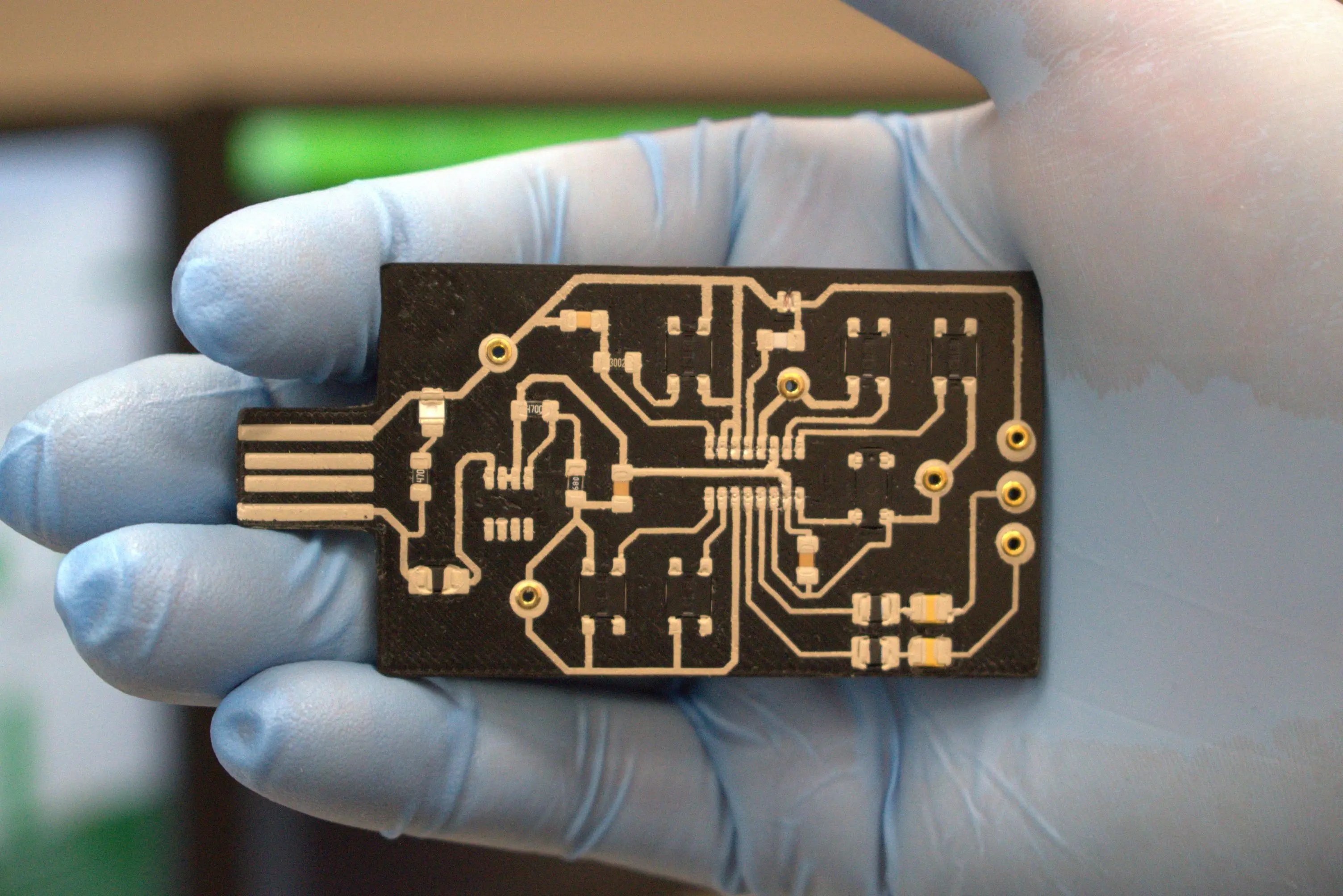
That's where this project started. A research team at the Faculty of Electrical Engineering at Czech Technical University in Prague, working with the University of Chemistry and Technology Prague, asked a question that might sound unlikely at first: could that waste become a printed circuit board (PCB)? Through the Sustainable Electronics Assembly Utilizing Plastic Waste (SELECT) project, the researchers demonstrated that it could. And the first working boards were made using the V-One PCB printer.
The problem with a conventional PCB
A conventional rigid PCB is typically made from FR4, a composite of woven fiberglass and cured epoxy resin. Copper traces are formed through processes such as etching and plating, and components are commonly attached using lead-free solder reflow at temperatures above 240°C.
These processes are well established, but they also make conventional PCBs difficult to recycle. FR4 cannot simply be melted down and reshaped. At the end of a board's life, it is typically shredded, and valuable metals can be recovered through pyrometallurgical or hydrometallurgical processes. The substrate itself, however, is largely lost. The wet chemistry involved in etching and plating also creates wastewater that requires treatment and contributes to the environmental impact of PCB manufacturing.
SELECT set out to replace this conventional process with something different: a thermoplastic substrate made from post-industrial waste, conductive traces deposited rather than etched, and components attached using conductive adhesives at temperatures low enough to protect the substrate.
Turning vinyl record waste into PCB substrates
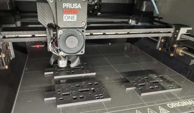
The recovered PVC/polyvinyl acetate (PVC/PVAc) compound is dried, extruded into 1.75 mm filament, and used to 3D print PCB substrates through fused deposition modeling (FDM). The material turned out to have a useful property that nobody had specifically engineered for: it is self-extinguishing.
The researchers found that printed specimens achieved a UL 94 V-0 flammability rating without added flame retardants. This is particularly noteworthy because many 3D printing filaments require additional flame-retardant additives to achieve the same rating. Mechanically, the printed substrate shows promising properties for rigid PCB applications, with a tensile strength of approximately 50-55 MPa and a Young's modulus of around 550-680 MPa.
But its glass transition temperature, around 72°C, is what shapes everything downstream. That temperature rules out conventional solder reflow and many standard curing schedules for conductive pastes, forcing the researchers to develop a low-temperature printing and assembly process.
After 3D printing, the substrates undergo thermocompression between sheets of polyester foil at 100°C and 50 N/cm² for five minutes. This helps reduce surface porosity left by FDM printing, giving the conductive material a smoother surface to adhere to.
Testing conductive materials with V-One
At the start of the project, the team had a substrate nobody had ever printed a circuit on, no idea which conductive paste would adhere to it, no idea whether a low-temperature cure would give usable conductivity, and no tooling. Screen printing — the process that the project eventually scaled to — is unforgiving at the prototyping stage: every layout change means a new screen, every paste trial means a full set-up, and what should be a five-minute experiment can turn into a week of work.
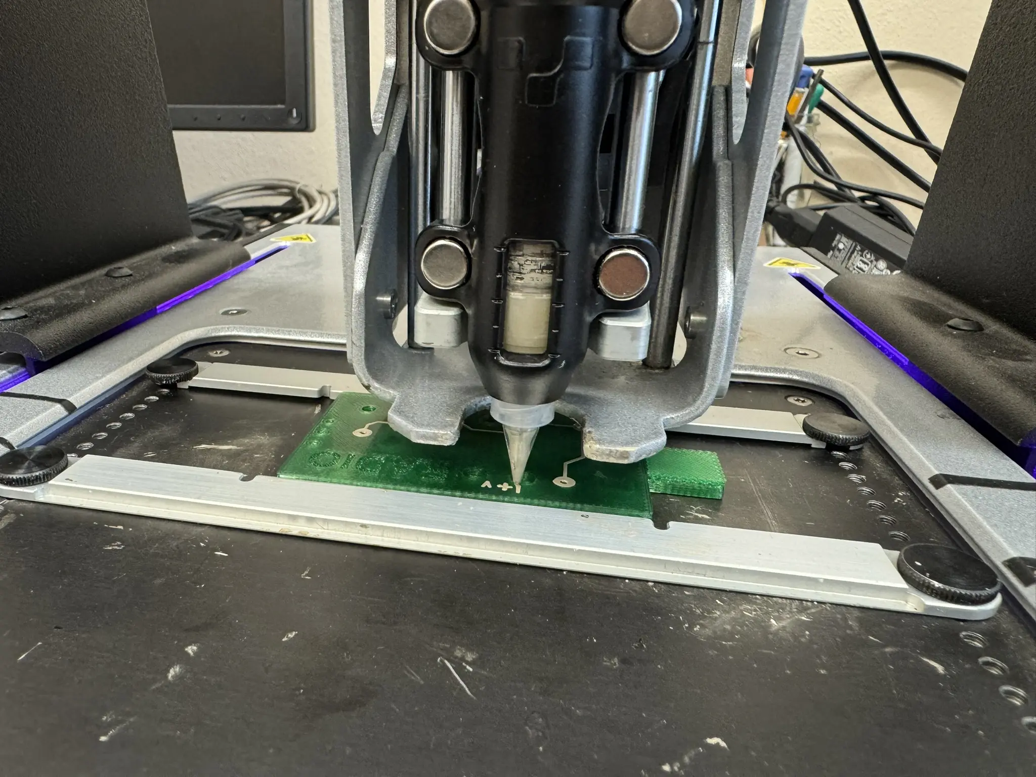
V-One removed that bottleneck. Direct ink writing meant the team could take a freshly printed, freshly planarised PVC/PVAc substrate, dispense a conductive pattern onto it, cure it on V-One’s heated bed at a temperature the substrate could tolerate, and measure its electrical properties that same afternoon. They could also change circuit layouts between samples without preparing new screens. The first functional demonstrator circuits built on recycled vinyl waste came off V-One, providing early proof that the approach was feasible.
V-One also produced the project's best measured conductor. Our Conductor 3 silver ink (since replaced by Conductor 4) achieved a sheet resistance of approximately 7 mΩ/□ at a printed thickness of around 50 µm — the lowest of all the silver-based conductive materials the team evaluated. By comparison, the screen-printing pastes used in subsequent pilot production achieved approximately 30-60 mΩ/□ under the tested conditions. Conductor 3 cured within the substrate's thermal limits and showed no observed compatibility issues with PVC/PVAc, unlike some of the other materials tested.
These findings mattered beyond the initial samples. They established a benchmark for evaluating the subsequent screen-printing process and demonstrated that the recycled substrate could support highly conductive traces. V-One remained in use throughout the project for verification samples and experiments that did not justify preparing a dedicated screen.
From prototyping to pilot production
The production process that grew out of those first trials keeps processing temperatures below 100°C. Conductive traces are screen printed, while the pads where components are attached receive a thicker deposit through stencil printing. This gives each joint the material volume it needs without making the traces unnecessarily thick.
Printing the substrate at 20% infill reduces warping at elevated temperatures, allowing the researchers to raise the conductive paste curing temperature to 70°C and improve conductivity. For double-sided boards, brass rivets installed using a hand lever riveter connect the two sides instead of plated through-holes. Nothing is etched, nothing is plated, and nothing is soldered.
Putting the process to the test: an FM radio, 84 years later
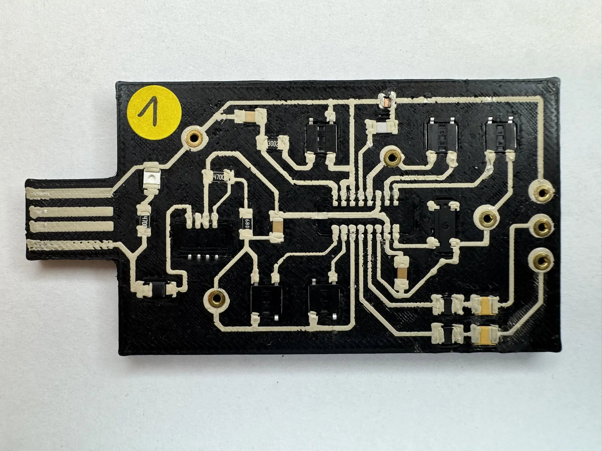
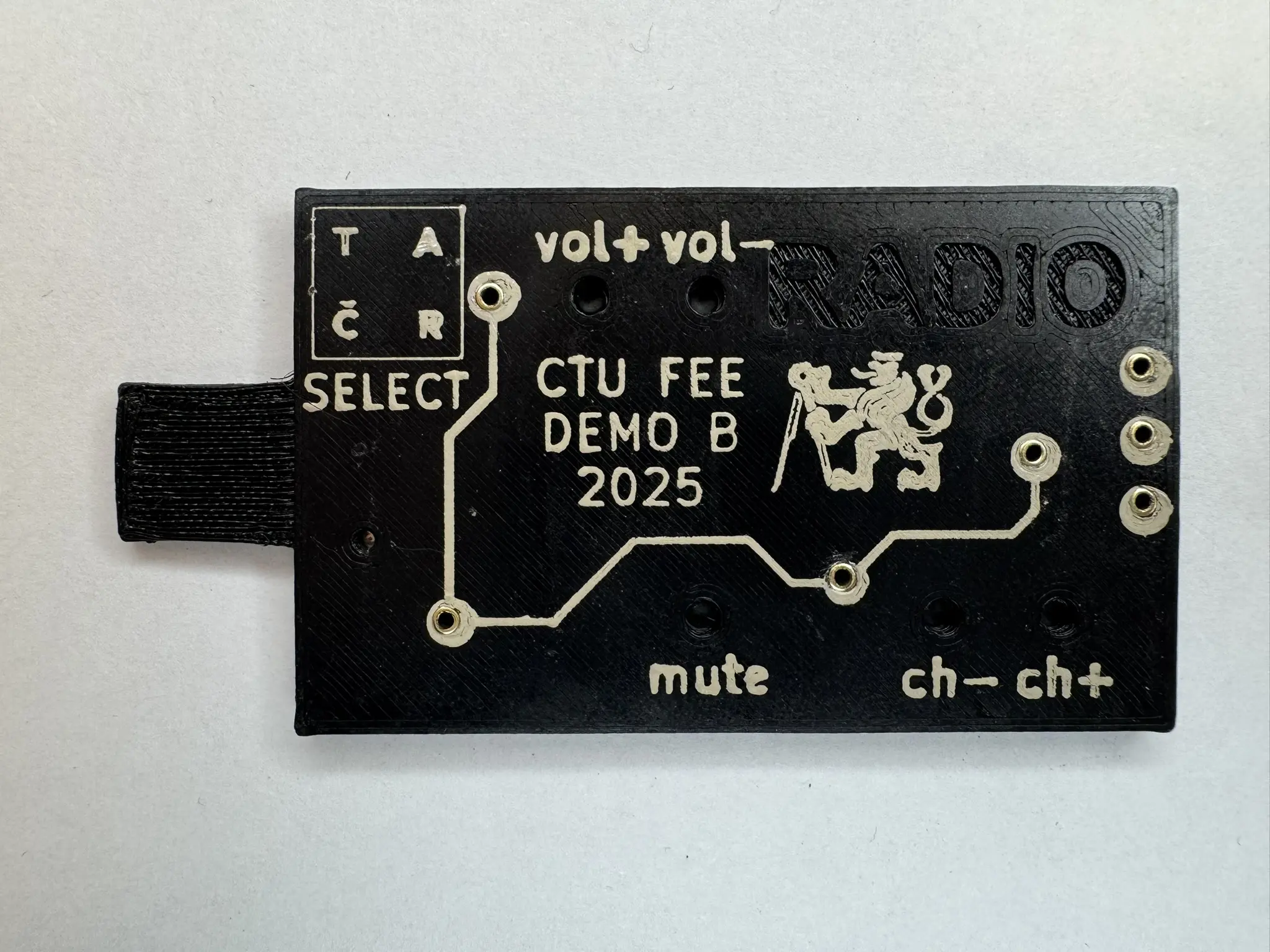
For the final double-sided demonstrator, the team chose an FM receiver built around an RDA5807FP chip, with 21 components mounted on both sides of the board. The choice was partly a nod to history: Paul Eisler, a pioneer of printed circuit board technology, developed an early printed circuit for a radio in the 1940s. More than eight decades later, the SELECT team returned to the radio, this time using a board made from recycled vinyl records.
The researchers built 20 FM radio units across two pilot batches. Testing showed a signal-to-noise ratio of up to 27 dB, with unit-to-unit variation below 4% within each batch. In parallel, a separate set of double-sided demonstrators underwent thermal shock testing, alternating between +50°C and −20°C for 15 minutes at each temperature.
After 1,000 cycles, 88% of the boards were still fully functional, with LED forward voltage and blinking frequency remaining stable throughout testing. The two failures were traced to identifiable process-related causes rather than the materials themselves. Together, these results show that the recycled substrate can support functional circuits and withstand repeated temperature changes under the tested conditions.
The environmental case
The SELECT team also evaluated whether the new manufacturing process offers environmental advantages over conventional PCB production.
A cradle-to-gate life-cycle assessment (LCA) compared the SELECT board against a conventional FR4 board of equivalent size and function. The results showed:
- Approximately 60% lower global warming potential
- Approximately 60% lower freshwater eutrophication
- Over 90% lower non-cancer human toxicity
Eliminating conventional etching and plating processes contributes to these reductions, particularly in environmental impact categories associated with chemical processing.
However, one material remains a significant contributor to the board's environmental footprint: silver. The conductive layer accounts for a substantial share of the total impact, which is why the researchers also developed a recovery route for the material. The recycled PVC/PVAc substrate can be ground and compression molded into a new sheet. Material degradation during this second processing cycle limits its potential applications, but it demonstrates that the substrate can be recovered and reused rather than simply discarded.
What comes next
SELECT is not aiming at high-volume PCB manufacturing, at least not yet. FDM printing of the substrate sets a practical limit on production volume. Instead, the immediate opportunity lies in prototyping and small-to-medium series production, where the ability to print, pattern, and assemble a PCB in one lab without a wet chemistry line offers clear advantages.
Screen and stencil printing are already established mass-production processes, so the main barrier to higher volumes lies in substrate manufacturing. Hot compression molding using dedicated tooling could provide a more scalable alternative.
The next challenge is the silver itself. Silver dominates both the cost of the finished board and its environmental footprint. Replacing it with copper-based conductive paste could improve both. However, the copper formulations tested so far have not delivered the conductivity or stability needed for practical use. Their electrical performance falls well below that of the silver pastes, and they degrade too quickly to be viable alternatives.
The good news is that the SELECT process does not depend on silver specifically. Screen printing, stencil printing, and low-temperature curing could also accommodate a suitable copper formulation, provided it meets the required electrical and processing conditions. Developing such a formulation could be an important next step toward reducing the cost and environmental footprint of these boards.
The self-extinguishing recycled filament also has potential beyond PCB substrates. Applications could include electronics enclosures, interior components, and HVAC parts — anywhere flame resistance without added flame retardants offers an advantage. The team is now exploring opportunities to commercialize both the recycled filament and the PCB manufacturing process.
Project facts
| Project | SELECT — Sustainable Electronics Assembly Utilizing Plastic Waste |
| Funding | Technology Agency of the Czech Republic, project no. SS07020107 (2024-2026) |
| Research partners | Czech Technical University in Prague, Faculty of Electrical Engineering; University of Chemistry and Technology Prague |
| Substrate | Recycled PVC/PVAc from vinyl record manufacturing |
| Voltera's role | V-One used for early feasibility testing, functional demonstrators, and ongoing verification |
| Best measured conductor | Conductor 3, approximately 7 mΩ/□ at 50 μm |
| Demonstrator | 20 double-sided FM radio units |
Exploring new possibilities for PCB prototyping
The SELECT project demonstrates that vinyl record manufacturing waste can be turned into functional circuit boards, opening up new possibilities for recycling industrial materials and rethinking conventional electronics manufacturing.
V-One helped make the initial experiments possible, allowing researchers to test conductive materials, refine their process, and produce functional prototypes before moving to pilot production.
It's a reminder that when researchers work with unconventional materials, having the right prototyping tools can make the difference between an interesting idea and a working circuit.
To learn more about the team:
- FMP group: LinkedIn
- Faculty of Electrical Engineering, Czech Technical University in Prague: LinkedIn
If you’re working on green electronics and would like to know how V-One can help, book a meeting with one of our technical experts.
Check out our customer stories
Take a closer look at what our customers are doing in the industry.