PWB vs. PCB in the Age of Additive Electronics
In the ever-evolving landscape of electronics manufacturing, terminology often carries hidden histories and technical nuances that shape industry practices. Two such terms — printed wiring board (PWB) and printed circuit board (PCB) — are often used interchangeably, but they represent distinct phases in the evolution of electronics.
While modern usage increasingly favors PCB as the catch-all term, comparing the difference between PCBs and PWBs in electronics reveals a fascinating journey from rudimentary electrical interconnections to today’s sophisticated, multi-functional electronic systems.
PWB and PCB: A historical and functional comparison
The terms PWB and PCB both describe non-conductive materials with conductive pathways, but they carry different historical and functional implications. Historically, PWB (printed wiring board) referred to boards with simple etched traces on basic substrates like phenolic paper, focusing solely on wiring connections. These were foundational in early electronics, such as industrial control systems, where basic interconnections were all that was required.
In contrast, the term printed circuit board emerged as the modern label for boards with more advanced materials, such as FR4 fiberglass, and designs that support features like multilayer routing, plated through-holes, and high-density interconnects. According to Wevolver, PCBs support advanced functionalities like multilayer board designs, signal integrity management, and thermal regulation, making them indispensable in modern electronic devices like smartphones and automotive systems.
| Aspect | PWB | PCB |
|---|---|---|
| Design | Single-layer, low-density traces | Multilayer, high-density routing |
| Typical materials | Phenolic paper | FR4 fiberglass |
| Applications | Legacy industrial systems | Modern electronics |
Even though the term PWB is still used in some regions — such as Japan — to avoid confusion with polychlorinated biphenyls (toxic chemicals), the term PCB is now the global standard for unpopulated circuit boards.
From bare boards to functional electronics: PCBA and packaging
The key difference lies not between PWB and PCB, but between bare boards (PWB/PCB) and assembled boards (PCBAs). While PWBs and PCBs serve as the foundation of electronic circuits, they remain non-functional until there are electrical components soldered onto them.
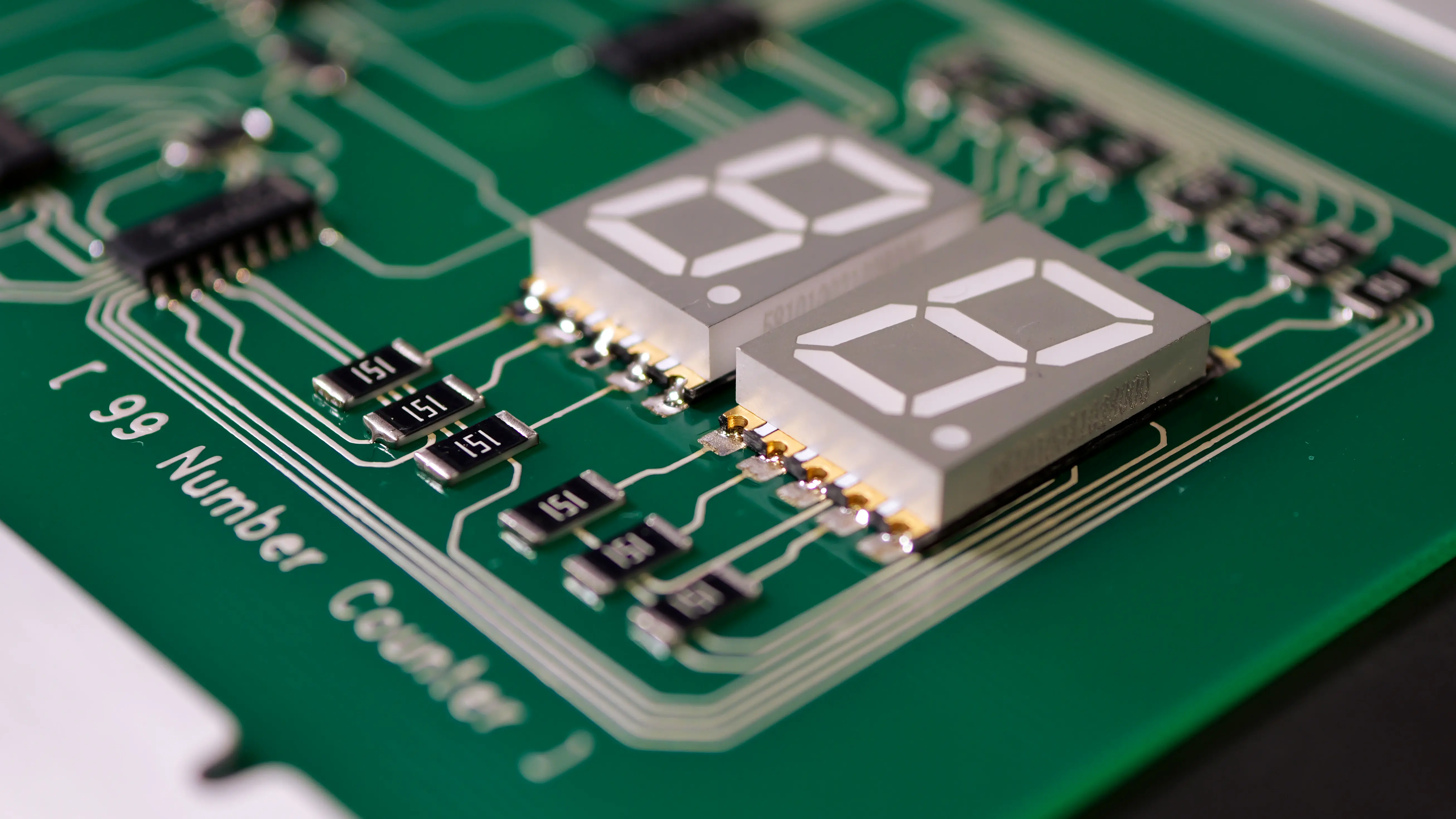
For example, the motherboard in a smartphone begins as a multilayer PCB substrate material. During PCB assembly, surface mount technology (SMT) streamlines the placement of tiny micro-components such as resistors, capacitors, and integrated circuits (ICs) onto the board’s surface. Reflow soldering then secures these essential components, bringing the PCB to life as a functional electronic system.
Beyond printed circuit assembly, advanced electronics packaging has further transformed how circuit boards function. Technologies like embedded component packaging (ECP) integrate passive components directly into PCB layers, reducing size while improving performance. Similarly, electroless nickel immersion gold (ENIG) finishes enhance electrical signal reliability and corrosion resistance, making PCBs more durable in high-performance applications like 5G networks, aerospace systems, and IoT devices.
The journey from simple PWBs to highly integrated PCBs and advanced packaging reflects how electronics have evolved from basic electrical connections to intelligent, high-density systems that power the intelligent era.
Rethinking the future of PCB fabrication with additive manufacturing processes
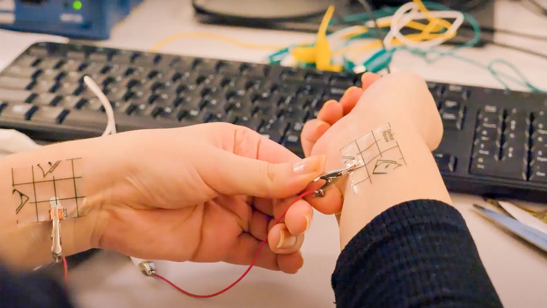
As electronics demand greater customization, miniaturization, and sustainability, additive manufacturing is redefining PCB fabrication. One such technology is direct Ink writing (DIW). Unlike traditional subtractive etching, DIW deposits conductive ink, dielectric ink, or other functional inks and pastes directly onto PCB substrates. This method significantly reduces material waste and enables rapid prototyping of complex geometries, such as stretchable surfaces for wearable devices.
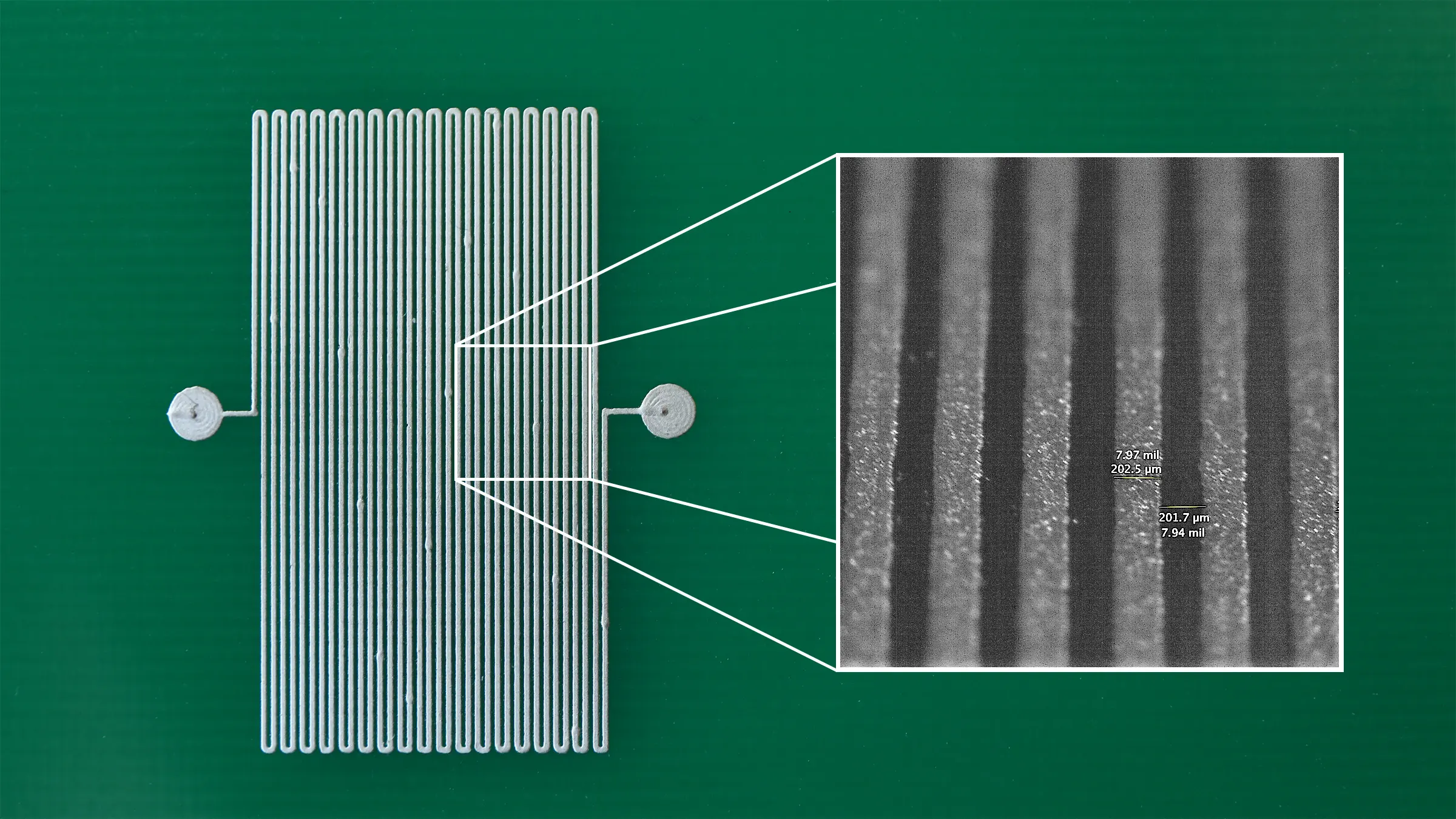
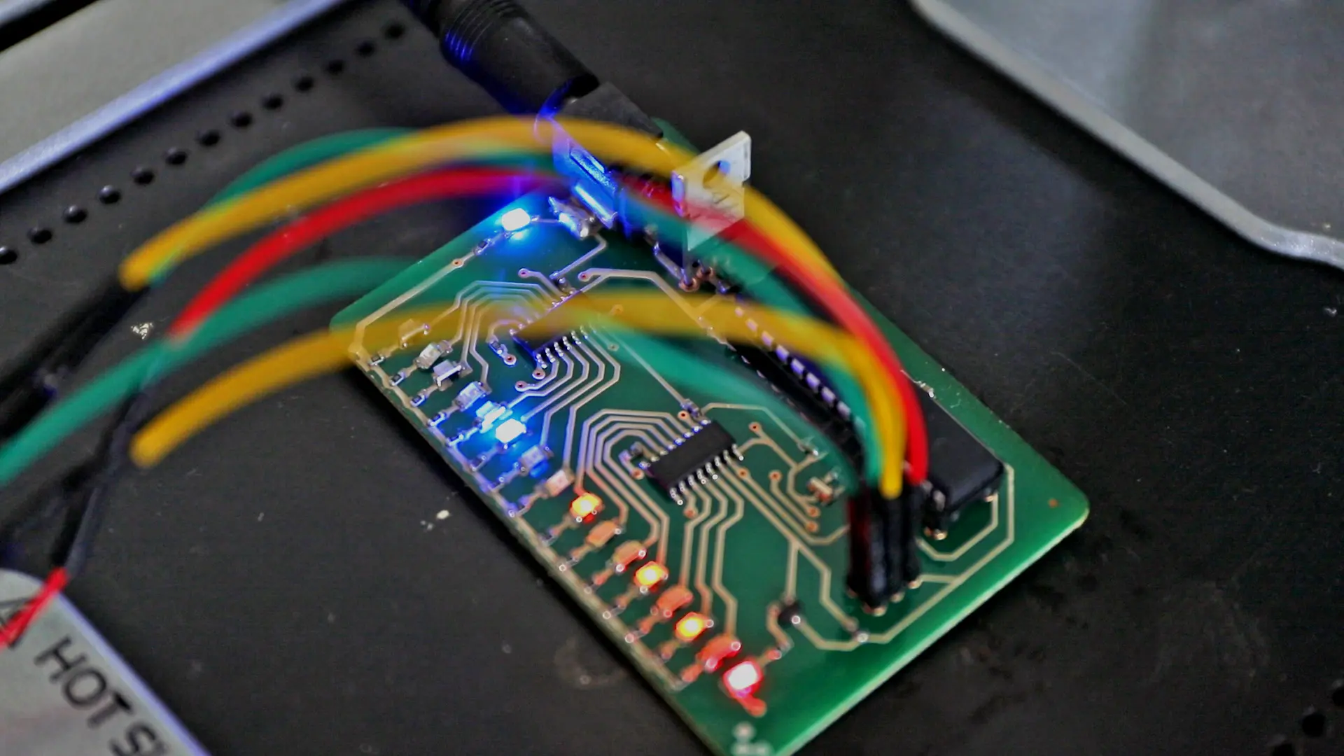
Even PCBA is evolving through additive techniques. Traditional PCBA relies on stencil printing, where a metal stencil is used to apply solder paste onto PCB pads before placing and connecting electronic components via reflow soldering. As such, it has several limitations, including the need for custom stencils for each printed board design, difficulty in handling fine-pitch components, and inefficiencies in prototyping or low-volume runs. DIW platforms such as Voltera’s V-One PCB printer and NOVA materials dispensing system can directly print solder paste onto PCB substrates, reducing the need for traditional stencils.
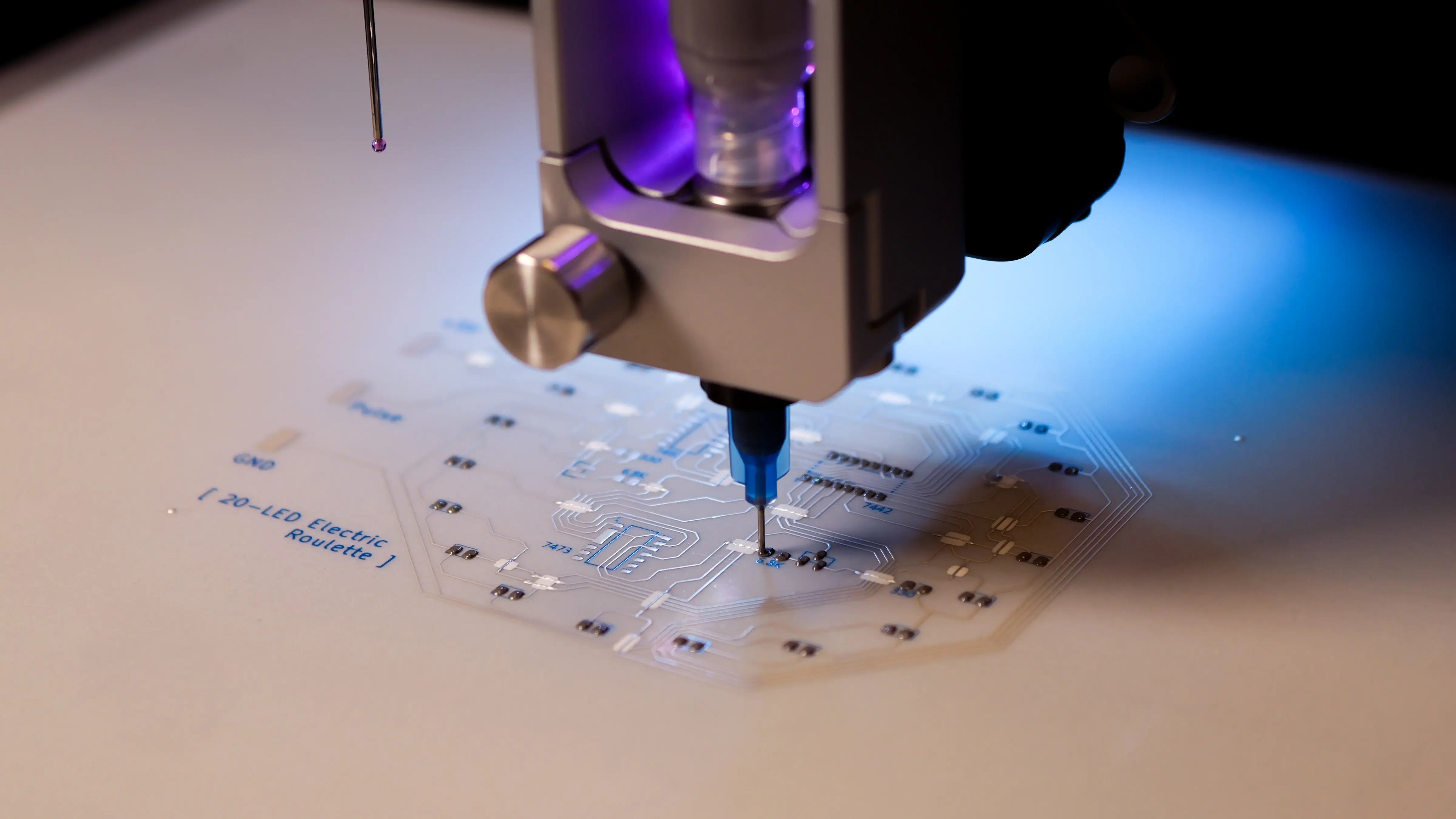
Researchers and developers have also explored embedding components during fabrication — a potential step toward merging fabrication and assembly into a single, seamless electronics manufacturing process. This shift could blur the lines between PCB fabrication and PCBA, leading to entirely new ways of designing and manufacturing electronics.
Conclusion
While the terms PWB and PCB reflect historical nuances in board fabrication, they both describe non-functional substrates — until PCBA brings them to life. But the shift from PWB to PCB wasn’t just about terminology. It reflected a major leap in how electronics are designed and manufactured, paving the way for more complex, high-performance systems.
Now, with the rise of PCB additive manufacturing, we are well on our way to another transformation — one that could merge PCB fabrication with PCB assembly. The fascinating journey of electronics is far from over. As we rethink legacy technologies and embrace new PCB manufacturing methods, the future of circuit boards will continue to evolve in ways we have yet to imagine, but one thing is for sure: the future is being built layer by layer.
Want to see our additive PCB prototyping projects? Check out these resources:
- Printing a Control Board for a Line Following Robot with Silver Ink on FR1
- Dispensing Solder Paste on Factory Fabricated PCBs
- Printing a Flexible PCB with Silver Ink on PET
And if you're curious about the latest Voltera content, don’t forget to subscribe to our newsletter!
Frequently Asked Questions
Can I create electronic prototypes using a printed wiring board (PWB) instead of a printed circuit board (PCB)?
Yes, if the design is simple. “PWB” historically meant a basic wiring board with conductive traces; for multiple layers, tighter spacing, and reliability across the entire board, modern PCBs are a better fit for most prototypes.
What’s the difference between PWB, PCB, and PCBA?
PWB is the older term tied to simpler, wiring-focused boards; PCB is the modern term for boards that support features like multiple layers and plated through-holes. PCBA is the board after attaching components, which is the version used in products.
Are additive manufacturing methods suited to consumer devices?
Additive methods shine for R&D, fast iteration, and short pilot runs. For high volumes in consumer electronics, mass production still favors etched laminates with copper traces due to cost and throughput.
Does additive PCB fabrication change the component mounting process?
You still apply solder to pads, place components, and reflow to form joints. What changes is the step before mounting: additive tools can dispense solder paste directly onto pads (including on prefabricated boards), enabling stencil-free assembly on early spins. That reduces setup time and can lower manufacturing costs while you iterate.
Check out our Customer Stories
Take a closer look at what our customers are doing in the electronics industry.
Check out our Customer Stories
Take a closer look at what our customers are doing in the industry.