How to Prototype PCBs In-House
Printed circuit boards (PCBs) serve as the “brains” behind nearly all electronic systems, from lighthearted pranks on package thieves to high-stakes carbon nanotube field-emission electron source. Fortunately, designing a PCB is more accessible than you might expect and does not require an engineering degree. The key is knowing how to begin with your circuit’s requirements and translate them into a prototype.
Requirement analysis and circuit design
Every PCB project begins with careful requirement gathering and circuit design. This involves determining the electrical needs (power levels, signal speeds, component types) and translating them into a schematic. Modern electronic design automation (EDA) software (e.g. KiCad, Eagle), also known as electronic computer-aided design (ECAD) software, makes it straightforward to draw schematics and lay out PCBs.

At this stage, you’ll need to capture the circuit logic in a schematic, design the PCB layout, and plan the placement of your conductive traces and components (e.g., adequate trace widths, component footprints, and clearances). Once the design is ready, it can be exported to standard Gerber files for PCB fabrication.
Constructing the circuit
For small-volume prototypes, you can either build the circuit on a breadboard or fabricate a PCB. The choice depends on factors like needed circuit complexity, frequency, durability, available tools, time, and budget. For more information on their differences, check out this article on breadboards vs. PCBs.
Breadboard prototyping
A reusable plastic board with spring-loaded contacts, a breadboard facilitates quick circuit assembly without solder. This temporary platform is invaluable for early testing and learning.
However, prototyping with breadboards comes with certain limitations:
- Parasitic capacitance and inductance in the wiring make it unsuitable for high-speed or RF circuits [1][2].
- Breadboards are designed for through-hole components, but as the industry moves towards surface-mount (SMT) packages, through-hole equivalents become harder to find and more expensive [1].
- Reliability issues can arise as contacts loosen or oxidize over time [1].
Additive methods for PCB prototyping
When looking for a more permanent and higher performance solution, custom PCB prototyping, particularly additive methods, becomes attractive.
Additive fabrication builds conductive patterns directly onto a substrate rather than etching or removing copper. This typically involves two steps:
- Printing conductive traces
- Curing conductive traces
In practice, creating additive PCB prototypes often means using specialized tools to directly print conductive material onto a substrate. A great example is a desktop direct ink writing (DIW) machine, like the Voltera V-One PCB printer.
It can dispense silver ink and solder paste on materials like FR1 and FR4, enabling both the creation of conductive traces and the assembly of components, all on one machine. Depending on design complexity, you can go from digital design to an assembled PCB in under an hour.
Benefits of additive PCB prototyping
- They achieve high accuracy for prototyping needs, resulting in comparable performance to a traditional etched board for practical purposes [3].
- You save precious materials since you only deposit material where needed.
- It is more eco-friendly and suitable for lab environments since you don’t need multiple baths of chemicals and don’t produce copper waste.
- If you are prototyping PCBs using novel materials on unconventional substrates, additive prototyping tools, like Voltera’s NOVA materials dispensing system, will better cater to your needs.
Investing in an additive tool makes the most sense if you’re prototyping PCBs in-house and need rapid iterations. However, if you’re a hobbyist who only builds circuit boards occasionally, additive methods may not be the most cost-effective option.
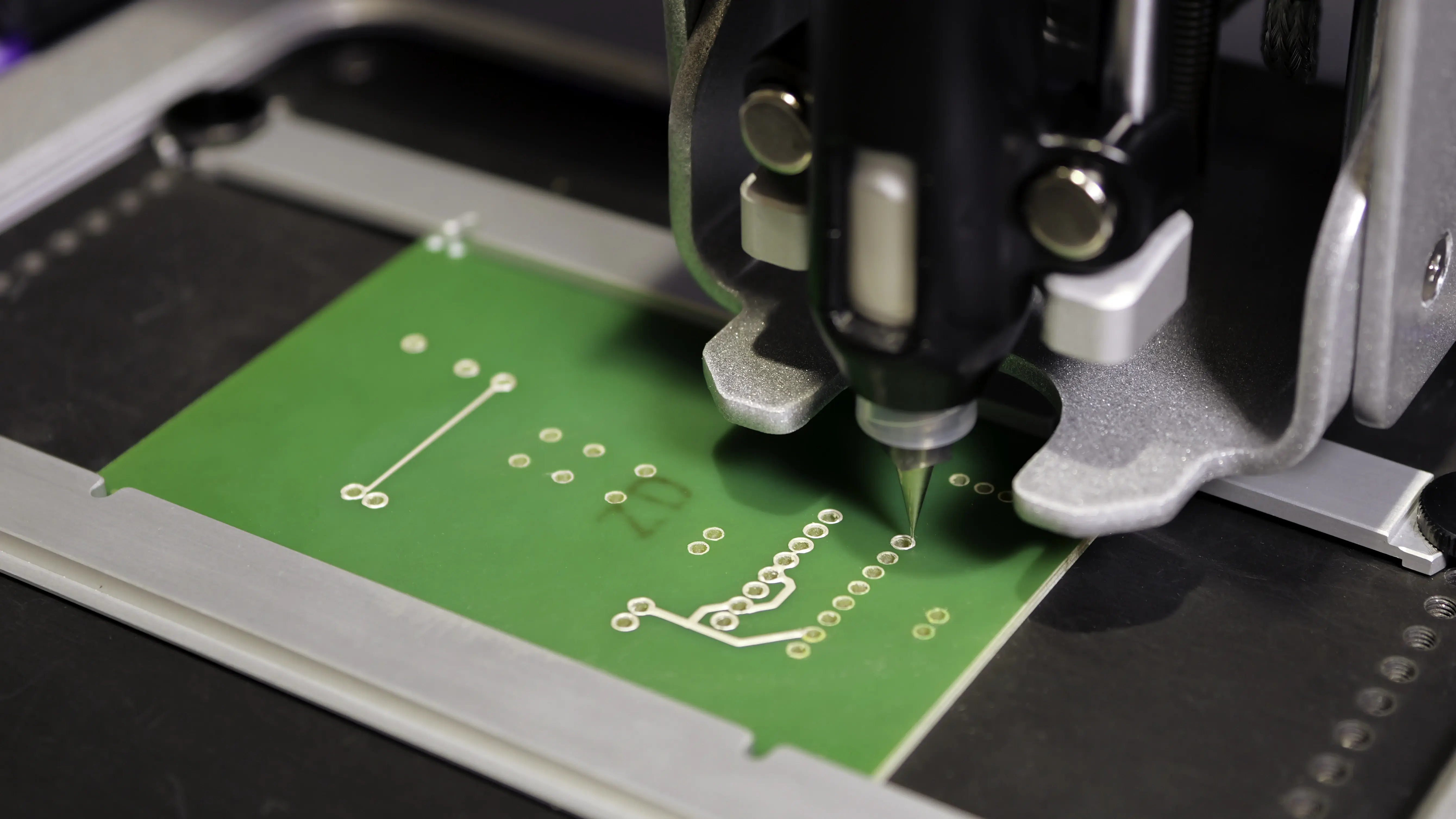
Subtractive methods for PCB prototypes
In small-volume contexts, many people create PCBs in-house using subtractive techniques, where copper is selectively removed or masked.
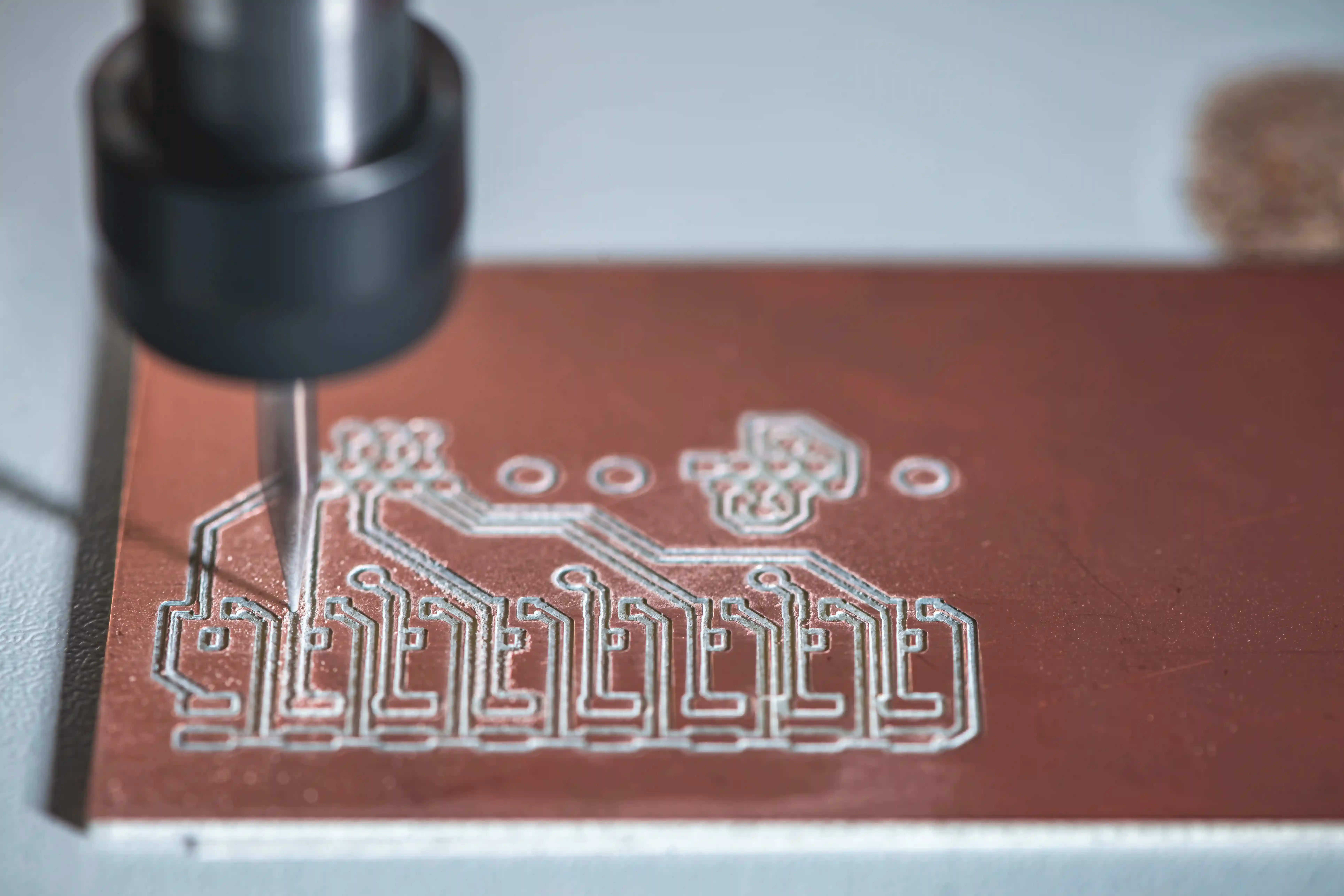
CNC milling uses a small desktop CNC router to physically mill away the unwanted copper from a copper-clad board. The ECAD design is first loaded into the CNC, which uses a very fine cutting bit to trace out the gaps between circuit traces, essentially carving out the circuit pattern from the copper layer. The result is similar to an etched board, but achieved by machining.
Pros
- CNC milling is quick for single boards. Once set up, you can get a finished board in under an hour, with no drying or chemical cleanup.
- Modern PCB mills can achieve decent resolution (e.g., a trace width of 0.3 mm).
Cons
- Very fine-pitch circuits or high-density boards may be challenging.
- The finish of traces is not as smooth as chemical etching.
- When setting up in an office or lab environment, you’ll need proper ventilation for hazardous dust.
Check out our comparison blog on CNC milling vs direct-ink-writing for PCBs for more information.
Laser printer toner transfer
This method uses a laser printer to create the circuit pattern. The PCB layout is printed in mirror image with toner onto a special paper substrate. This print is then placed toner-side down on the copper board and heated (using a clothes iron or laminator) to re-melt the toner, which then adheres to the copper.
After cooling, the paper is soaked and peeled off, leaving the black toner pattern stuck on the copper as an etch resist. The board is then etched in acid, which removes copper except under the toner traces.
Pros
- It is one of the fastest ways to construct a circuit in-house.
- With practice, trace widths around 0.15 mm are feasible.
- It’s a low-cost technique and doesn’t require special chemicals beyond common etchant.
Cons
- The process can be unreliable. Success depends on many variables such as paper type, toner brand, iron temperature, pressure, and timing.
- For double-sided boards, aligning the two layers is tricky.
Photolithography
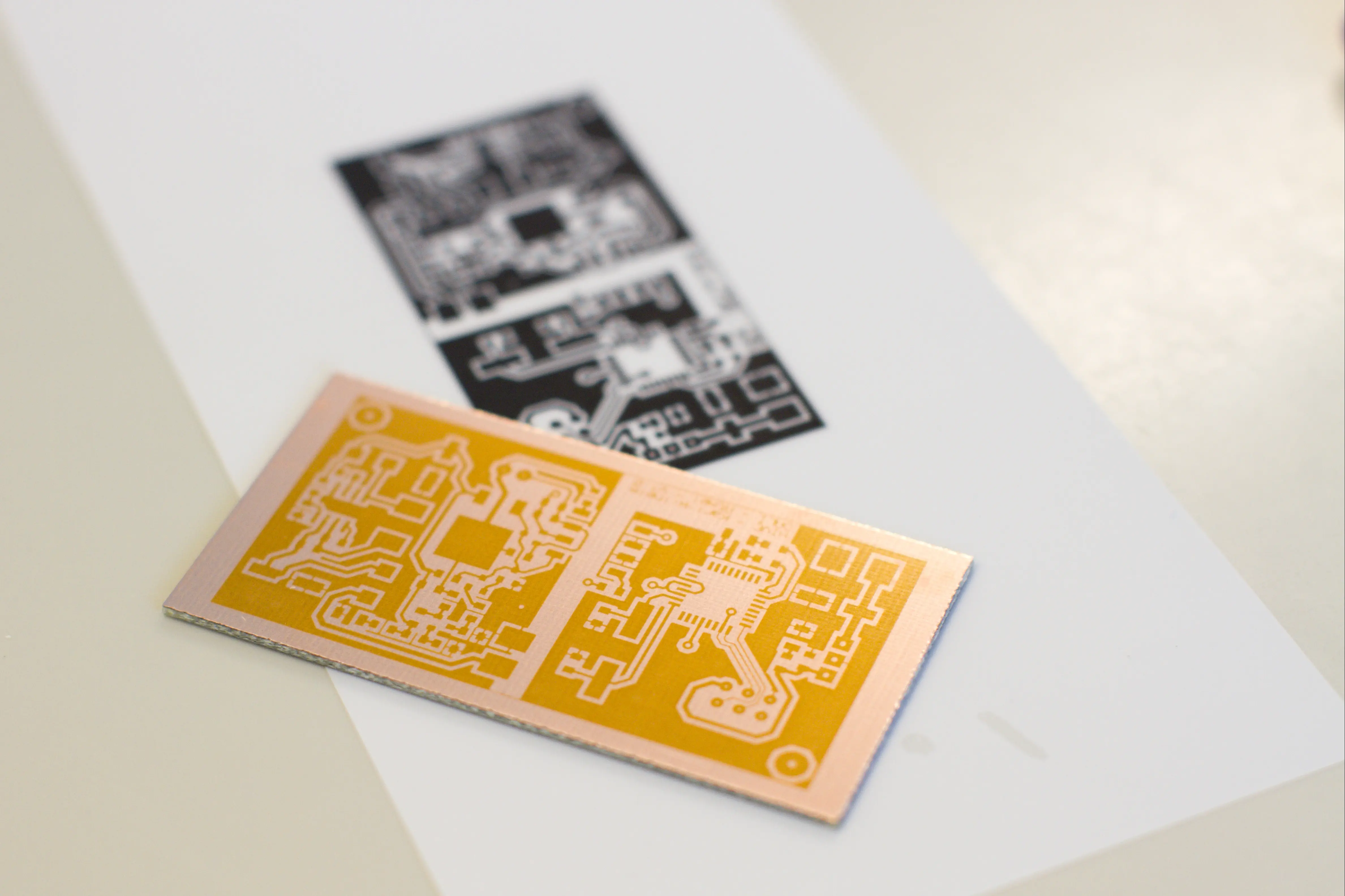
Also known as ultraviolet (UV) photo-etching, this method uses photosensitive PCB boards, a type of copper boards pre-coated with a light-sensitive resist layer. The PCB pattern is printed in black onto clear transparency film using a laser printer or photoplotter. The transparency is placed over the photosensitive board and exposed to UV light. Where the black ink blocks the UV, the underlying resist stays unexposed and will later protect copper; where transparent, the resist hardens.
After exposure, the circuit board is developed in a chemical developer, washing away the unexposed resist and revealing a precise copper pattern ready for etching. Etching then removes the bare copper, as usual, and finally the remaining hardened resist is stripped to leave the finished copper traces.
Pros
- Photo-etching can achieve finer traces and spacings.
- It’s suitable for more complex circuits and yields repeatable results if the process is well-calibrated.
Cons
- The process involves more steps and chemicals. Beginners must handle timings and development carefully — under- or over-exposure can ruin the pattern.
- It has a more stringent requirement of the setup environment — a completely dark workspace for handling the unexposed boards.
Post-processing
No matter how the PCB is made, whether by etching, milling, or a DIW machine, after fabrication you have a bare board that needs to be populated with components to become a working circuit. The assembly steps typically involve:
- Drilling (if double-sided or multilayer)
- Soldering and reflowing
- Testing for connections, continuity, and shorts
- Final touches like mounting enclosures or coloring
Conclusion
Making PCBs for in-house prototyping involves a mix of planning and choosing the right construction method. Breadboards offer a quick reality check for simple ideas, but for a robust and final-feel prototype, learning how to make custom PCBs, especially using additive manufacturing technologies, will be invaluable.
Interested in learning more about PCB prototyping? Check out these resources:
- Application: PCB Prototyping
- Customer story: Revolutionizing PCB Design Education with V-One
- Video: Printing a Decimal Counter Circuit with Silver Conductive Ink on FR1
- Blog: 3D Printing vs. PCB Printing — What’s the Difference?
Want to make PCB prototypes with V-One? Book a meeting to speak with one of our technical representatives.
References
[1] Verbelen, Y., Belle, D. V., & Tiete, J. (2013). Experimental Analysis of Small Scale PCB Manufacturing Techniques for Fablabs. International Journal of Engineering Innovation & Research. 2(2), 136–143. https://www.researchgate.net/publication/268078465_Experimental_Analysis_of_Small_Scale_PCB_Manufacturing_Techniques_for_Fablabs.
[2] Scherz, P., & Monk, S. (2016). Practical Electronics for Inventors, Fourth Edition. O’Reilly Online Learning. https://www.oreilly.com/library/view/practical-electronics-for/9781259587559/.
[3] Rao H. C, Varaprasad, B. K. S. V. L., & Goel, S. (2021). Direct Ink Writing as an Eco-Friendly PCB Manufacturing Technique for Rapid Prototyping. 2021 Fourth International Conference on Electrical, Computer and Communication Technologies (ICECCT), 1–7. https://doi.org/10.1109/icecct52121.2021.9616903.
Check out our Customer Stories
Take a closer look at what our customers are doing in the industry.