Webinar Recap: Scaling Printed Electronics from Lab to Fab
Getting a printed electronics prototype to work in the lab is hard. Getting it to work reliably, repeatedly, and at scale is a completely different challenge, and one that trips up research teams, startups, and industry groups alike.
In this webinar, Katarina Ilić, nanotechnology engineer and co-founder of Voltera, walked through why the lab-to-fab gap exists, how common tool choices shape (or limit) path to production, and designing for scale from the start.
If you missed it, here's what you need to know.
Why scaling printed electronics is so hard
The printed electronics market is growing fast, from $17.76 billion in 2025 to a projected $105.86 billion by 2034, at a 22% compound annual growth rate (CAGR). Healthcare, wearables, energy harvesting, and biosensors are all driving demand. And generative AI is beginning to show up in printed electronics workflows, helping teams optimize designs and reduce material waste.
But development timelines haven't kept pace with market enthusiasm. It still takes an average of 5-7 years to move a new printed electronics technology from R&D into production, and profitability takes even longer.
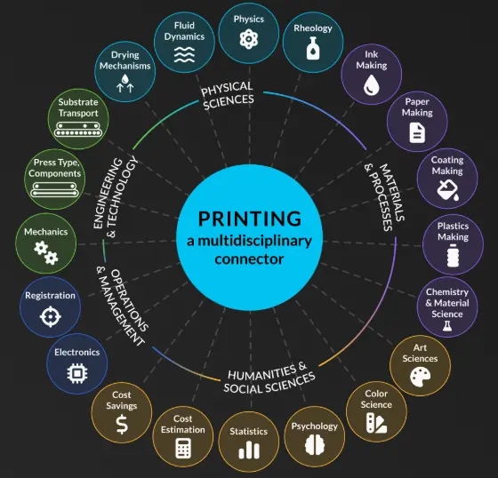
Part of the reason is that printed electronics sits at the intersection of so many disciplines: fluid dynamics, rheology, chemistry, material science, mechanics, electronics. In the lab, you tune one variable at a time. In production, all of those variables have to be understood together and controlled reliably.
To scale printed electronics, as a result, requires knowing which parts of your lab process will survive contact with manufacturing.
The lab-to-fab gap is fundamentally a process problem
One of the key points Katarina made in the webinar was regarding what the gap actually is.
A device can perform well under controlled lab conditions and still be very far from a scalable process. The questions change as you move through development stages:
- Lab success: Can I print this structure and validate the materials?
- Development success: Can I repeat and improve this device?
- Production success: Can this process be transferred, controlled, and scaled at reasonable cost?
These stages sound like natural next steps, but the movement between them isn't. A working prototype does not automatically contain a manufacturing process inside it. And if the tool used to prove out the concept doesn't connect to future manufacturing processes, teams can find themselves starting over. As a result, the earlier you start asking "what am I learning from how I'm making this?", rather than just "can I make this?", the smoother that transition will be.
The ink is the design system
Before comparing technologies, Katarina explained how engineers should approach printed electronics development: the ink as the design system.
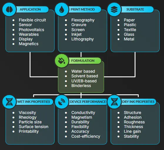
Formulation controls wet ink behavior, which then controls printability. Dry film properties control adhesion, conductivity, thickness, and durability. All of that feeds into device performance. A material that looks great in a vial isn't automatically a printable ink. A printable ink for one process isn't automatically transferable to another. And an ink that produces a clean-looking pattern isn't automatically reliable over the device's lifetime.
Before locking in a process, it's worth asking:
- Does the binder adhere to the target substrate?
- Does the solvent damage previous layers or interact with equipment?
- Does the ink fit within the downstream printing method's rheology window?
- Can it cure within the substrate's thermal budget?
- Does the final film meet conductivity, thickness, flexibility, and stability targets?
- Is the material cost and waste profile viable at scale?
The three common lab tools and where each fits
Katarina explained how each tool has a material window, a resolution window, an iteration cost, and a relationship to production. And the right question isn't "which tool is best?" but "what do I need to learn right now?"
Inkjet
Inkjet (specifically piezoelectric drop-on-demand) is one of the most widely used tools in printed electronics research. It's digital, precise, and great for fine-featured work with small amounts of material. It's particularly well-suited for formulation screening, fluid-substrate studies, and thin-film applications like OLEDs, photovoltaics, and organic transistors.
The constraint with inkjet, is that inks must stay within a narrow jetting window defined by viscosity (typically 1-30 cP), surface tension, and density. Functional solids have to stay below roughly 30% by volume to maintain reliable jetting, which means inkjet doesn't deliver the thick, high-loading films that many demanding applications require.
Inkjet does have a scale-up path: flexographic roll-to-roll printing works well for applications like NFC antennas, where features are larger and integration is simpler. But for more complex flexible hybrid electronics (FHE) devices, biosensors, or energy storage applications, the process translation isn't direct. The ink chemistry is fundamentally different from screen printing, and teams often have to reformulate significantly.
- Best for: Formulation screening, fluid and substrate studies, fine-feature patterning, thin-film applications
- Less suited for: Thick-film applications, high-current devices, or anything that needs to scale via screen printing without major reformulation
Screen printing
Screen printing uses a pre-tensioned mesh and squeegee to push paste through patterned openings onto the substrate. Each material and each layer gets its own screen. It handles high-viscosity pastes (1,000 to 1,000,000+ cP), deposits thicker functional layers (typically 10-35 µm), and works with conductive, dielectric, resistive, and encapsulant materials.
The biggest advantage for scaling: material continuity. The pastes used in screen printing prototyping are often the same materials used in production. That means less reformulation risk when transitioning.
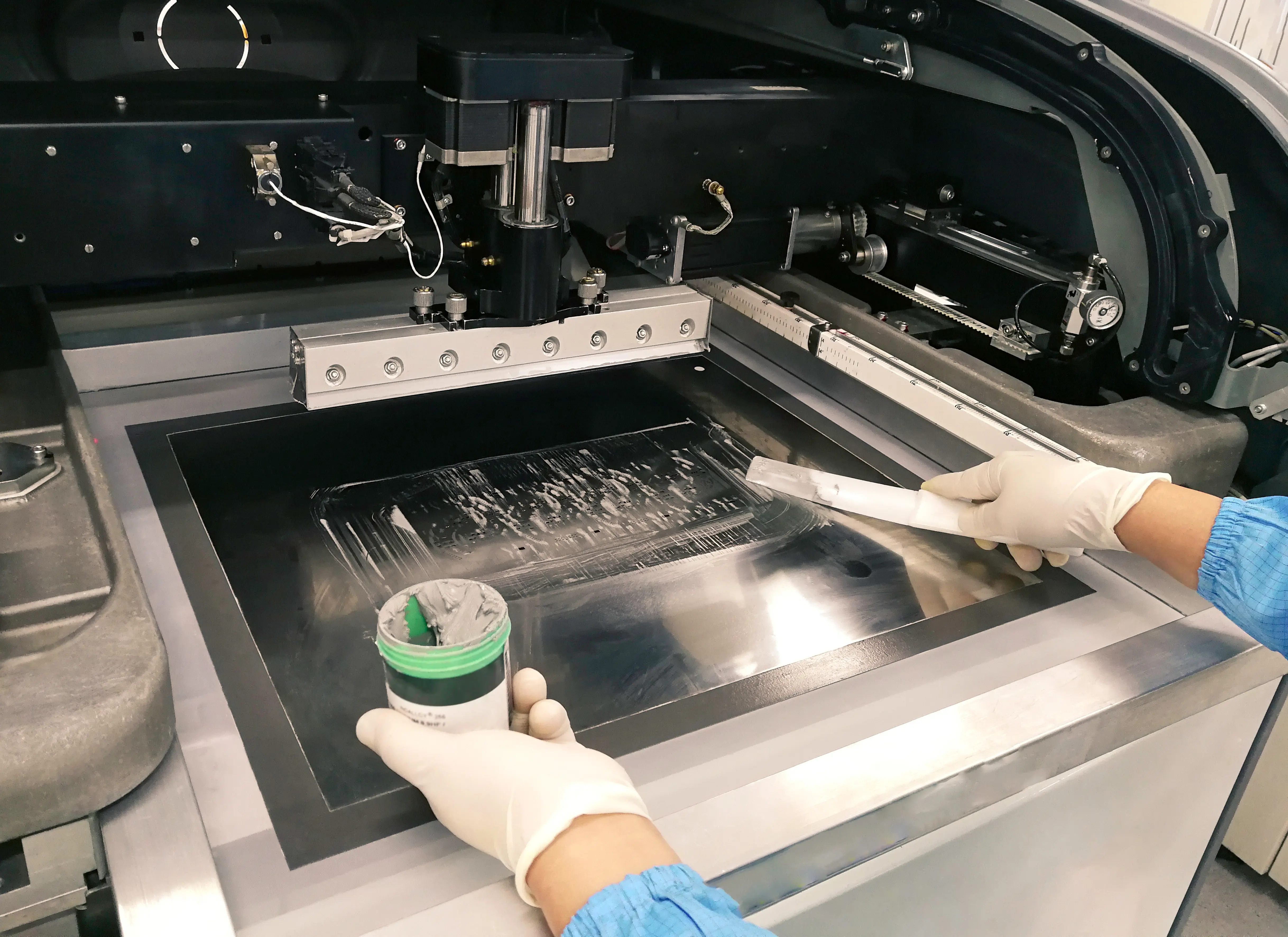
However, screen printing is far less forgiving during iteration. The screen itself isn't a passive stencil: mesh count, wire diameter, tension, emulsion thickness, and particle size all interact, and getting a new screen every time you change the design introduces new variables that make it hard to tell whether results are driven by the material or the tooling change.
The hidden cost of trying again adds up quickly: tooling costs, setup and cleanup labor, delays between design changes, material waste, failed prints, and lost learning cycles.
- Best for: Stable paste-based designs heading toward high-throughput production
- Less suited for: Early-stage, high-iteration development where materials and geometries are still in flux
Direct ink writing (DIW)
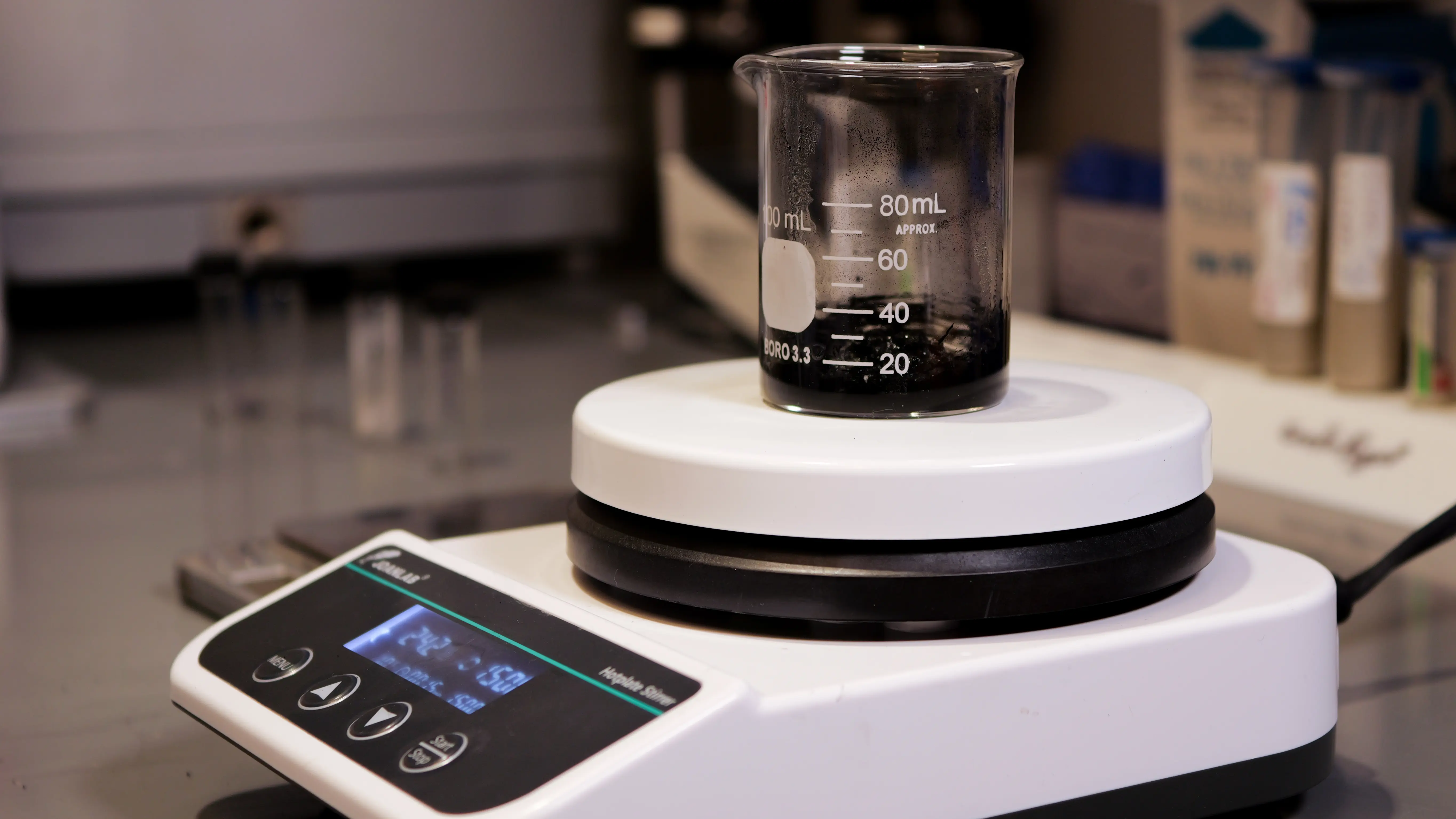
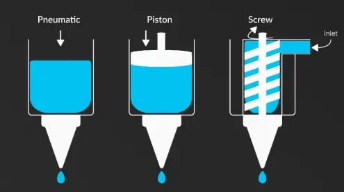
Direct ink writing deposits a continuous line of material along a digitally controlled toolpath, no screen or stencil required. The flow is driven pneumatically or by positive displacement.
The material regime is what makes DIW particularly valuable for lab-to-fab workflows: it operates in the thick-film paste regime — the same viscosity range and material chemistry used in screen printing. Functional solids can be loaded up to 95% by weight. These are shear-thinning materials, meaning they flow under pressure from the nozzle and quickly recover their shape on the substrate.
Because DIW uses production-relevant materials, the learning transfers more directly. Post-processing physics (curing, sintering, shrinkage, porosity) behave similarly between DIW and screen printing. Design rules, such as minimum line/space, overlap, registration tolerances, translate more readily too.
It's not a perfect transfer (screen printing applies higher shear forces, which affects particle packing and film density), but the underlying material behavior is much closer than what you get when translating from a low-viscosity process.
- Best for: Rapid iteration on designs while staying close to production-relevant materials and processes
- Less suited for: High-volume, quick-turn production
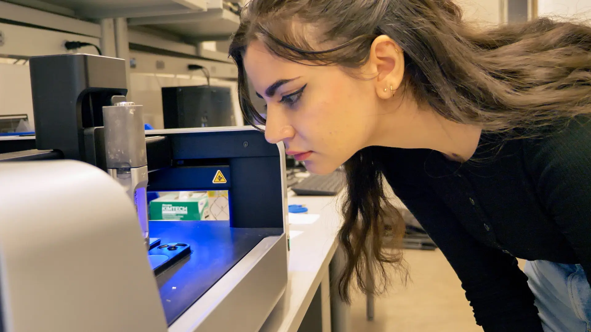
Where NOVA fits
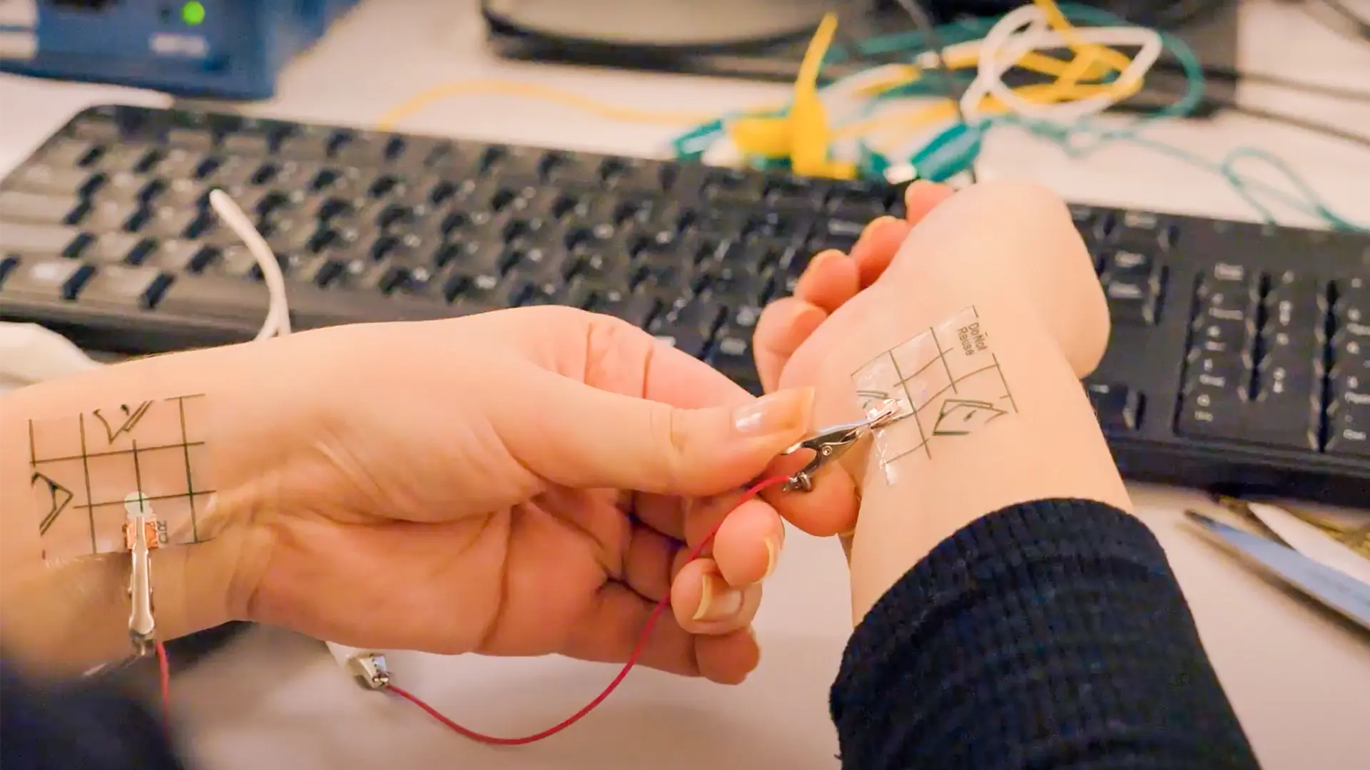
NOVA is Voltera's direct ink writing system for prototyping flexible hybrid electronics, and it's designed specifically for the development gap — the stage before the production line where teams need to move fast without drifting away from manufacturable materials.
With NOVA, you can change circuit geometry without ordering a new screen, print high-conductivity materials and solder paste, test adhesion across different substrates, and work with materials that behave like what you'll use at scale. Features like an augmented reality overlay for circuit repair, printing conductive ink precisely over damaged traces can also be of practical use in rapid iteration cycles.
It won't replace screen printing in production, but prototyping with NOVA makes your path to screen printing faster, repeatable, with fewer dead ends.
Research spotlight: Printed glucose biosensors
Katarina then introduced a recent research example that illustrates how process choice connects to real-world constraints, not just device performance.
The research question was “can single-use glucose biosensors be redesigned so that silver and gold can be recovered and reused, while still maintaining functional sensor performance”?
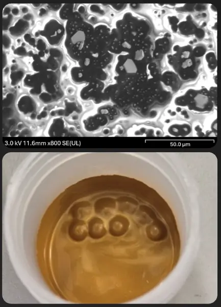
The team developed silver and gold inks with selective solvent compatibility — the binders could be dissolved later to recover the metals cleanly. For fabrication, they used a hybrid approach: screen printing for high-coverage silver tracks, and Voltera's direct ink writing platform for targeted gold deposition in precision regions.
After use, the recovered Ag/Au was reformulated into second-generation inks and used to fabricate new devices that maintained the same functional performance.
The results were striking:
- 82 wt% reduction in material use compared to screen printing alone
- €823.20 in savings per 1,000 prints
- Life cycle assessment (LCA) showed substantial reductions across most environmental impact categories
This example demonstrates what it looks like to design a process with the full development chain in mind — from ink formulation and deposition method, all the way through recovery, cost, and lifecycle impact.
Live Q&A
Q: Can you create prototypes on an inkjet system and then move them to screen printing for production?
A: It's possible, but Katarina cautions against it. The fundamental chemistry of inkjet materials is very different from screen printable pastes. If the plan is to scale via screen printing, start working with screen-printable materials in the lab now. Don't optimize for inkjet and then try to translate.
Q: Is DIW suitable for manufacturing, or mainly prototyping?
A: Mainly prototyping, for now. Current DIW tools on the market aren't designed with the repeatability, tolerance, and throughput requirements of production.
Q: Can NOVA be used for circuit board repair?
A: Yes, in some cases. NOVA has a repair feature that uses an AR workflow to map board features and deposit conductive ink along damaged traces. The constraint is resolution — the system operates reliably at around 100 µm trace widths, so highly dense boards may not be a fit.
Q: Have you worked with PEDOT:PSS paste on NOVA?
A: Yes — in collaboration with Polytechnique Montréal, Voltera achieved some of the finest resolution seen with that material: around 80 µm features. Reach out to sales@voltera.io for more details and the published work.
Q: What about ink ordering and print-as-a-service?
A: Conductive inks are available through Voltera's store. We also offer a print-as-a-service option through its in-house materials science team, who work with customer-supplied samples.
Additional resources
Want to learn more about scaling printed electronics? Check out these blogs:
- NOVA vs. Screen Printing — ROI for FHE Prototyping
- Inkjet vs. Direct Ink Writing (DIW) for Printed Electronics
- Screen Printing vs. Direct Ink Writing for Printed Electronics
Ready to talk about how NOVA can help your project scale? Book a meeting to speak with one of our technical representatives.
Check out our Customer Stories
Take a closer look at what our customers are doing in the industry.