NOVA vs. Screen Printing — ROI for FHE Prototyping
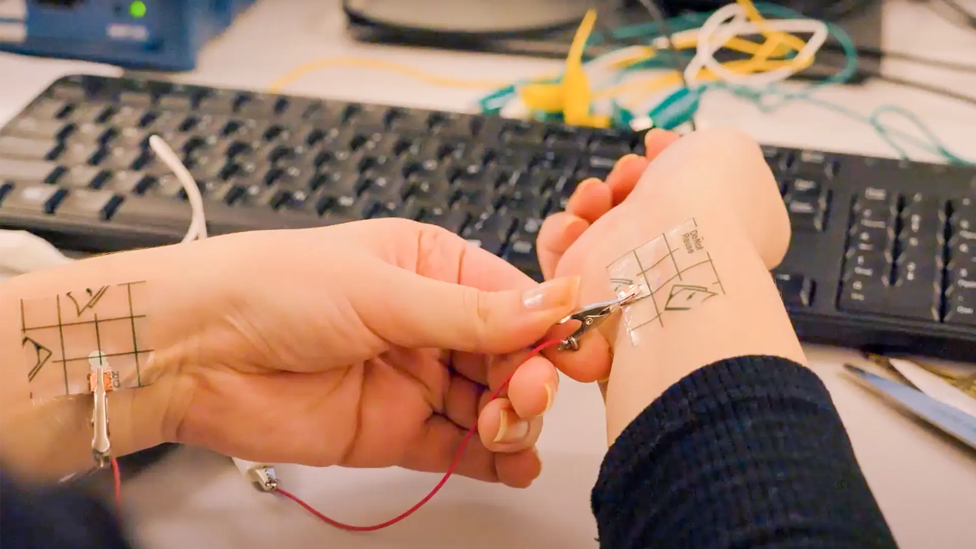
Rapid prototyping in flexible hybrid electronics (FHE) demands tools that enable fast design iteration, novel material experimentation, and high design flexibility without the overhead of full-scale manufacturing. To maximize return on investment (ROI), it’s essential to choose an option that aligns with your specific prototyping needs.
How screen printing works
Screen printing in electronics is a contact deposition process that uses either a mesh screen or a metal mask (a stencil with pre-etched apertures) to transfer ink onto a substrate. If you’re using a mesh screen, areas corresponding to the circuit pattern are left open while other areas are masked with an emulsion before printing.
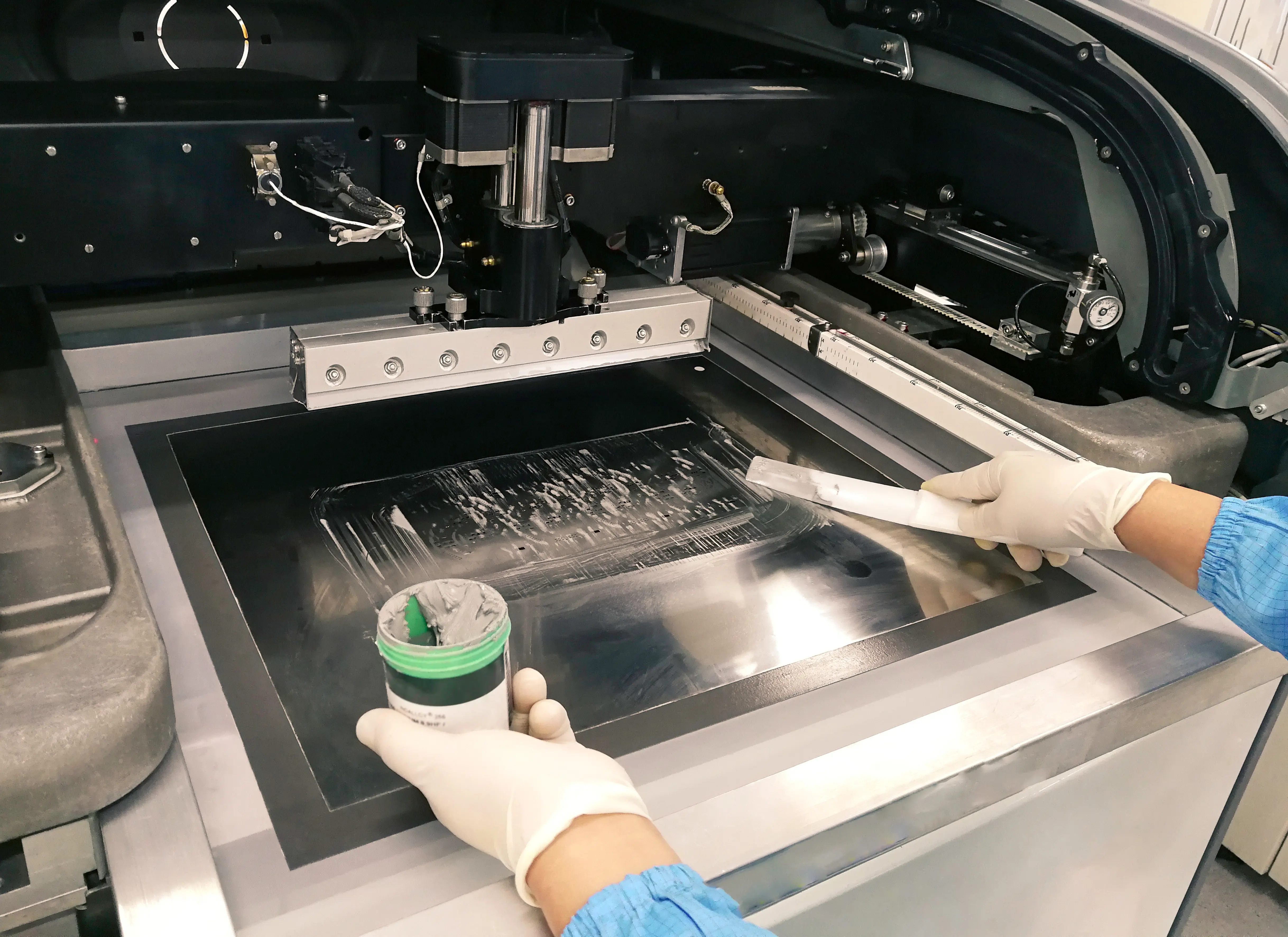
During printing, a conductive or functional ink is poured onto the screen and a squeegee wipes across it, pushing ink through the open areas onto the substrate beneath it. The substrate is then heated or UV cured to solidify the ink or paste and ensure conductivity.
Screen printing supports a wide range of materials, such as conductive ink, dielectric ink, and solder paste. It can also print on a variety of flexible substrates, including polyethylene terephthalate (PET), polyimide, textiles, and even paper or curved surfaces [1].
How NOVA works
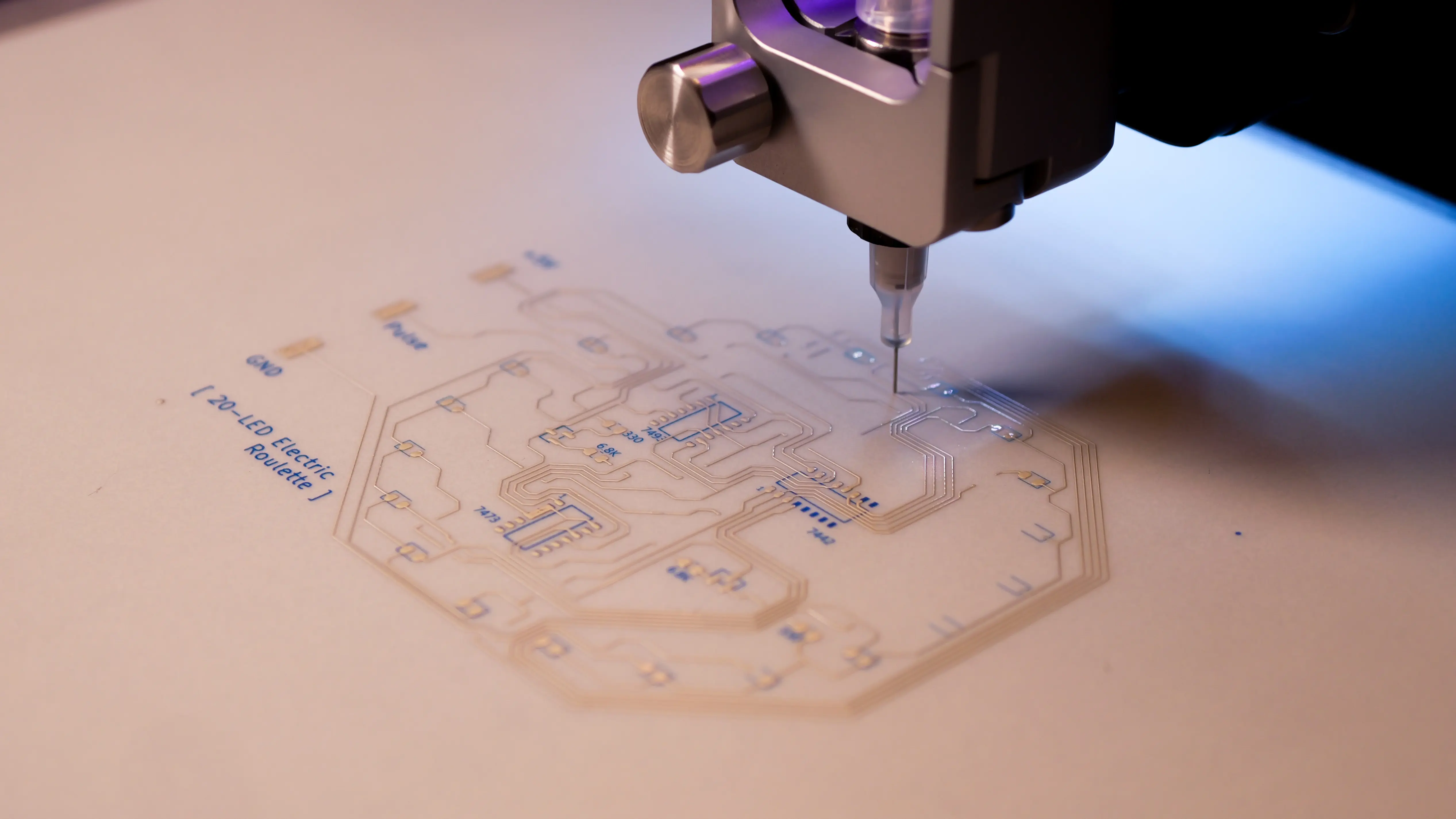
Voltera’s NOVA is a materials dispensing system that uses direct ink writing (DIW) to print flexible circuits layer by layer, without any screens or stencils. It dispenses functional inks and pastes through a nozzle, creating the desired pattern under digital control.
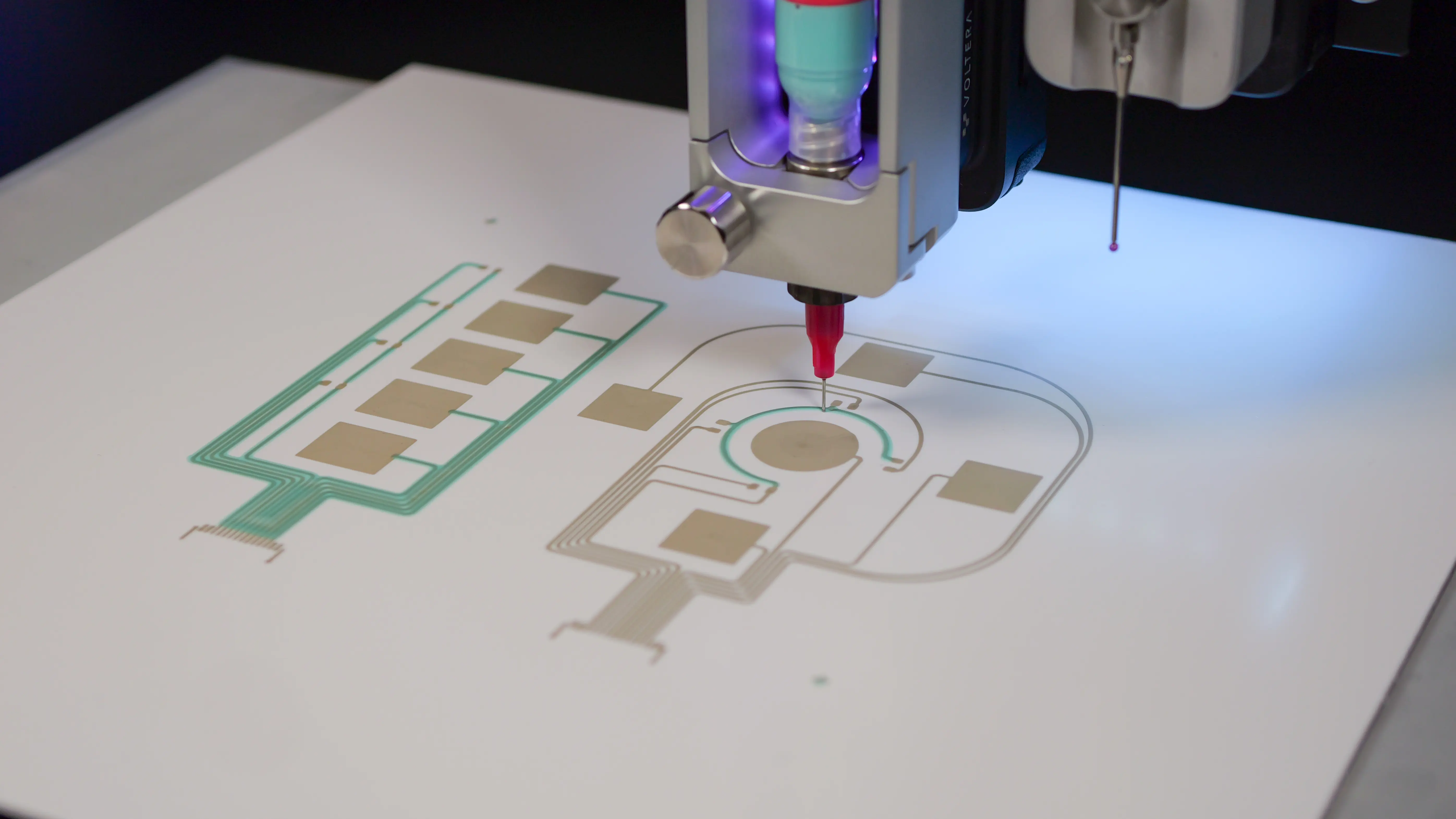
In practice, the user loads a syringe of the chosen material, mounts the substrate on the print bed (a vacuum table that holds flexible films flat), and uploads a digital design — Gerber file or SVG (beta) — for the machine to print. Like screen printing, the pattern must then be cured to become conductive.
The materials NOVA can dispense largely overlap with screen-printable materials, as do the compatible substrates. However, in a prototyping environment, these two methods differ significantly in terms of ROI and overall agility.
NOVA vs. screen printing for prototyping
For engineers developing FHE devices, the key ROI question is usually not which method has the lowest theoretical unit cost at scale. It is which method makes it easier and more economical to keep iterating while the design is still changing. In prototyping, every revision can trigger new setup work, new material consumption, and new opportunities for delay. That is where the economics of screen printing and NOVA begin to diverge.
For the sake of illustration, this comparison assumes a high-iteration prototyping scenario totaling 1,000 prints across development. Under those conditions, screen printing carries recurring costs that grow with each design change: new stencils, material waste, setup effort, and manual labour. NOVA, by contrast, shifts more cost upfront but lowers the recurring cost of each additional prototype cycle by removing the need for stencils and reducing setup friction.
Material cost
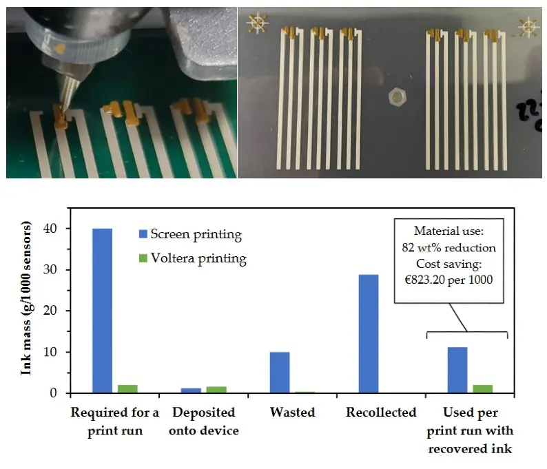
Material efficiency is one of the clearest differences between stencil-based and direct ink writing workflows. In a 2026 study comparing screen printing with Voltera’s direct ink writing printer for biosensor fabrication, the authors reported an 82 wt% reduction in material use and €823.20 in cost savings per 1,000 prints with Voltera printing [2] . While this study used V-One rather than NOVA, it illustrates a broader prototyping principle: when material is deposited only where needed, waste can fall substantially compared with screen-based transfer methods. For teams working with costly functional inks, that difference compounds quickly over repeated iterations.
Stencil and consumable costs
Stencil-driven workflows also carry a recurring tooling penalty. With each design tweak, whether it is a size change, a layer adjustment, or a material-specific revision, a new stencil may be required. Using the estimate cited here of $109 to $362 USD per stencil, 100 iterations would translate to $10,900 to $36,200 USD in stencil costs alone, assuming one new stencil per iteration. NOVA avoids that recurring cost because the pattern is generated digitally rather than through a physical screen or stencil.
Labour costs
Labour is another meaningful driver. Screen printing requires more manual setup, handling, monitoring, and cleanup, and may also introduce coordination work around stencil sourcing and changeovers. By contrast, NOVA reduces much of that process overhead through a software-driven workflow. Using a median hourly rate of $50/hour for mechanical engineers in the US, even a modest reduction in labour per iteration can add up quickly over a long development cycle.
For example, if NOVA saves one hour per iteration, then 100 iterations would reduce labour cost by about $5,000. If the savings are closer to 0.5 hours per print, then across 1,000 total prints the savings would be about $25,000. The exact number depends on whether labour is being modeled per print or per iteration, so that unit should be stated explicitly.
To summarize the ROI implications: NOVA carries a higher upfront equipment cost, but it reduces the recurring cost of prototyping by removing stencil remakes, reducing wasted material, and lowering manual setup effort. Screen printing can remain compelling when a design is stable and volumes are high, but during development, when teams are still learning and revising, the cost of trying again often matters more than the nominal cost of any single print. That is where NOVA tends to deliver stronger ROI.
Conclusion
It should be noted that NOVA and screen printing are complementary, rather than strictly competing in the overall development pipeline. NOVA fills the prototyping and innovation gap, empowering rapid design cycles and material innovation without worrying about production logistics. Screen printing then takes over for manufacturing scale-up, offering low unit costs for large runs. As NOVA is compatible with most-screen printing materials (1,000-1,000,000 cP in viscosity), teams using NOVA for prototyping can seamlessly scale into production. This way designers get the best of both — agility upfront, efficiency later.
Interested in learning more about NOVA and screen printing? Check out these resources:
- Blog: Introduction to Screen Printing
- Blog: Screen Printing vs. Direct Ink Writing for Printed Electronics
- Webinar: Printing Multilayer Flexible And Stretchable Circuits
Need a customized calculation of the ROI of your current workflow? Book a meeting to speak with one of our technical representatives.
References
[1] Wiklund, J., Karakoç, A., Palko, T., Yiğitler, H., Ruttik, K., Jäntti, R., & Paltakari, J. (2021). A Review on Printed Electronics: Fabrication Methods, Inks, Substrates, Applications and Environmental Impacts. Journal of Manufacturing and Materials Processing, 5(3), 89. https://doi.org/10.3390/jmmp5030089.
[2] Stobo, A.-M., Izquierdo-Bote, D., Bernard, L., Hampton, K., Wolfe, N., Parker, A., García, M. B. G., Villasuso, I. Z., Stockill, B., Ioannidis, R. O., Bikiaris, N. D., Robinson, P., Richardson, S., Maxfield, J., Gill, L., Peavoy, G., Moliner, E., & Lamming, G. (2026). Closing the Loop: Sustainable and Cost-Effective Glucose Biosensors Through a Circular and Digital Design. Electronics, 15(4), 796. https://doi.org/10.3390/electronics15040796.
Check out our Customer Stories
Take a closer look at what our customers are doing in the industry.