Inkjet vs. Direct Ink Writing (DIW) for Printed Electronics
In printed electronics, two additive technologies often come head-to-head: direct ink writing (DIW) and inkjet. They are both digital and don’t require additional tooling for design changes, but they tackle different ends of the printed electronics spectrum. DIW delivers robust, real-world functional prints — thick, conductive, and reusable with minimal hassle. Inkjet, by contrast, supports high-precision, low-power electronics that are cost-sensitive.
How they work
Direct ink writing
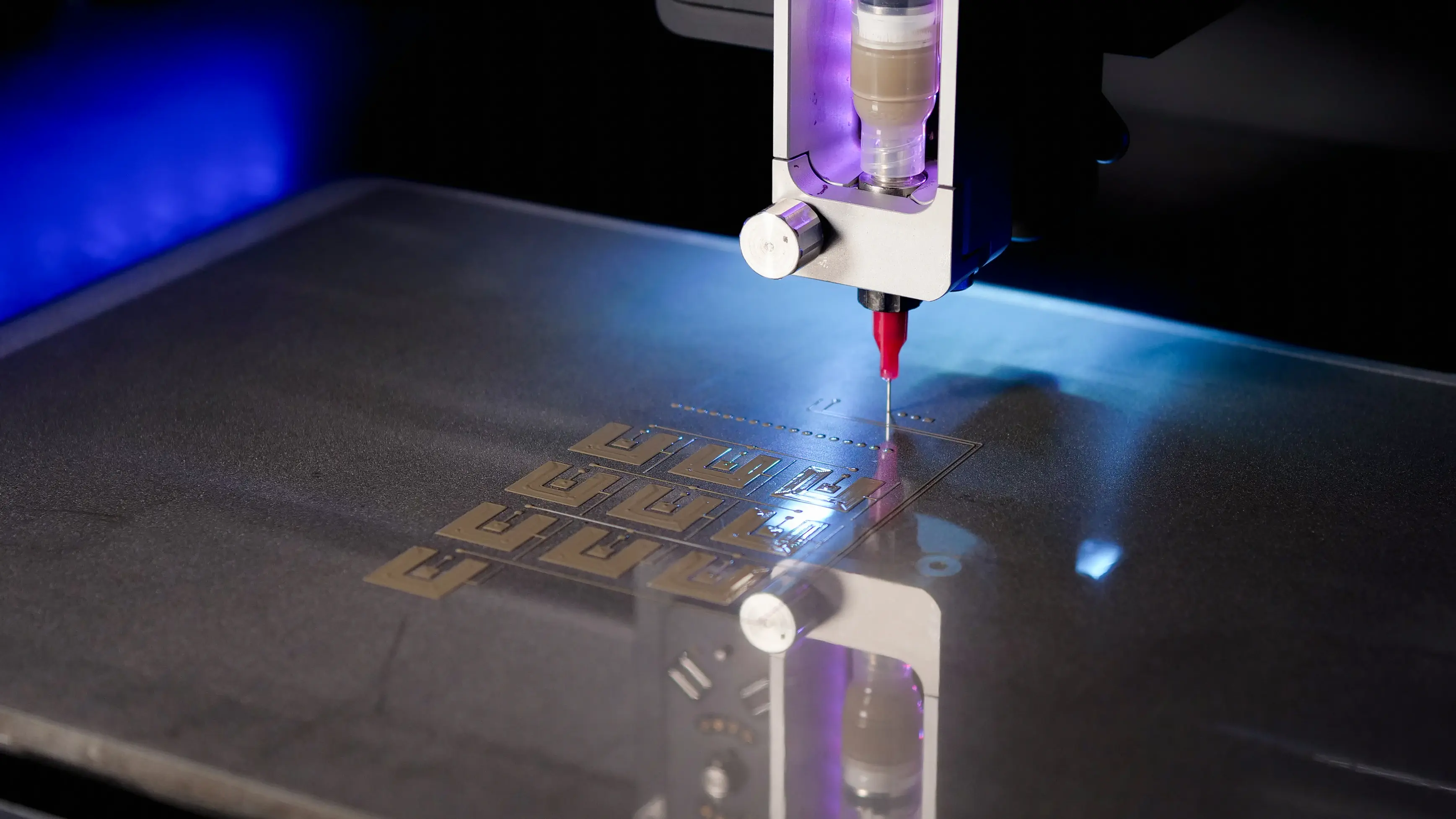
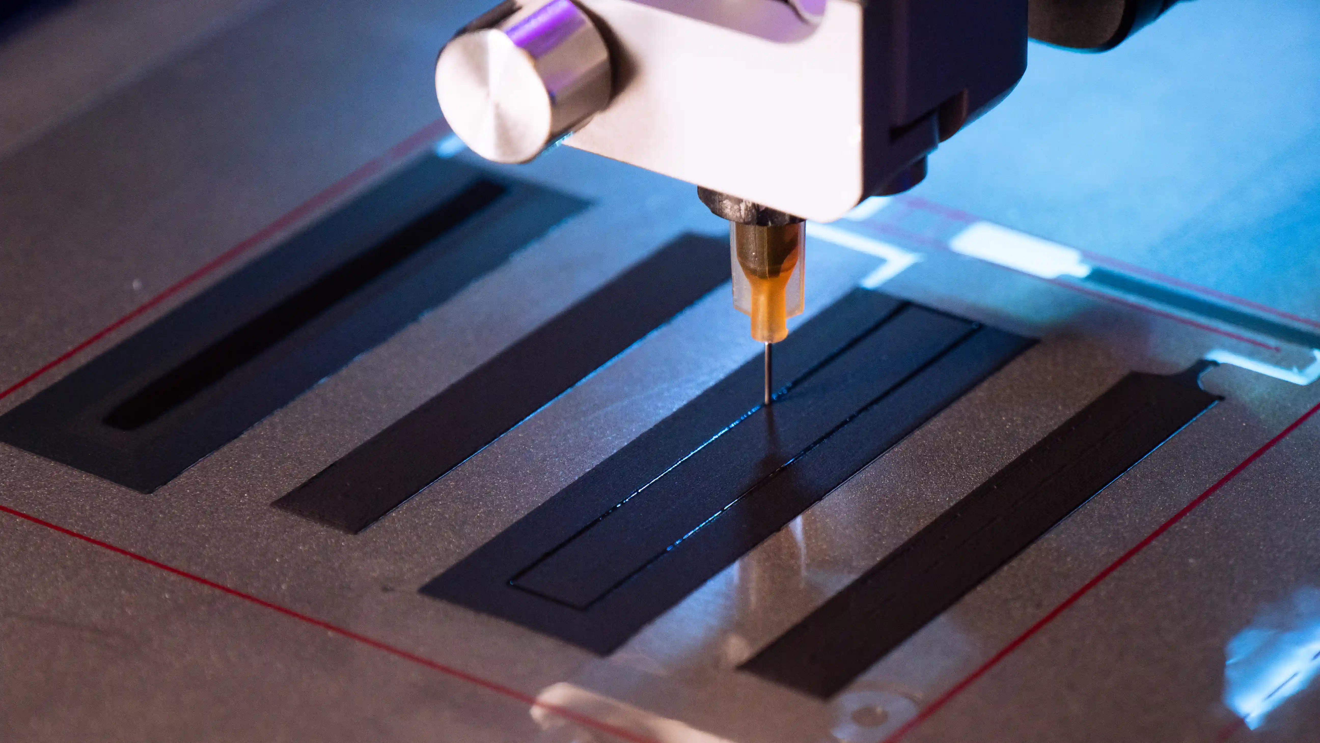
DIW is a digitally driven extrusion process where a precision syringe deposits high-viscosity conductive inks and functional materials layer by layer, following a programmed toolpath. The dispensing unit may use pneumatic pressure, a piston, or a screw-driven system. DIW supports a broad range of materials, from metal-rich pastes and polymers to ceramics and composite inks [1].
Inkjet
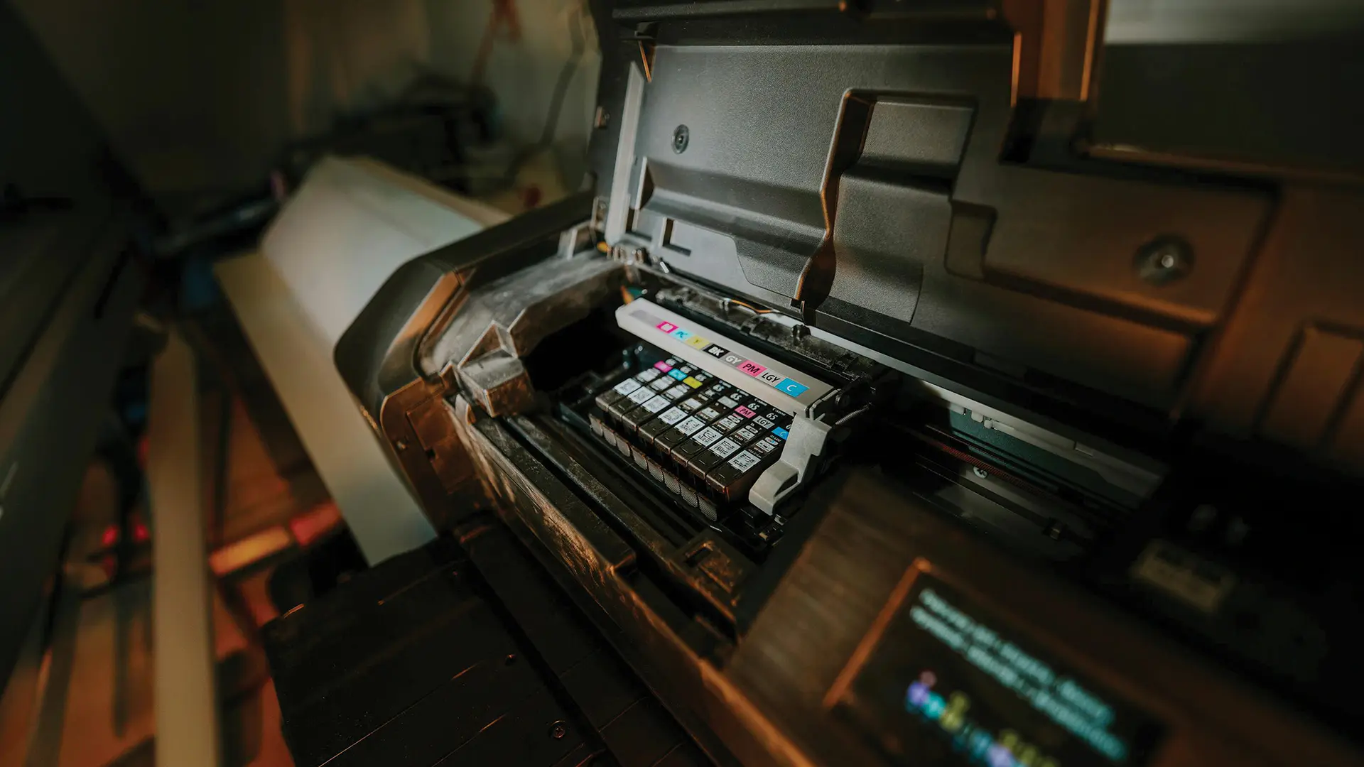
Inkjet systems eject tiny droplets (typically 0.5-100 pL) of low-viscosity nanoparticle inks via their nozzles, typically driven by piezoelectric actuators. The technology offers ultra-fine resolution, but inks must meet stringent formulation rules: low viscosity (<30 cP), surface tension ~28-42 dynes/cm, and chemically stable particle suspensions.
Key differences between direct ink writing and inkjet
| Criteria | Direct ink writing | Inkjet |
|---|---|---|
| Typical metal loading | 80-90% by weight (>50 vol%) | 20-40% by weight (typically <30 vol%) |
| Achievable conductivity | ~10⁷ S/m or higher (≥10× that of most inkjet formulations) | ~10⁵-10⁶ S/m |
| Layer thickness | Thick layer (up to 70 μm) in one pass with high-energy density | Thin layers (typically 0.5-1.5 μm) with limited conductivity unless layered |
| Solderability | Compatible with low-temp alloys | Not suitable with most formulations |
| Material range | Broad:
| Narrow: Solvent-based, low viscosity (<30 cP), low-surface-tension (28-42 dynes/cm) fluids |
| Ink sourcing flexibility | Open platform: wide range of third-party or custom inks | Proprietary or vendor-locked inks recommended; tuning is difficult |
| Post processing | Typically low-temperature cure (room temp to 150°C); options for photonic/thermal | Often requires sintering or photonic curing to achieve conductivity |
| Mechanical strength | Strong adhesion and durability | Less robust and prone to breakage |
| Substrate compatibility | Flexible and rigid, more forgiving with varied substrate chemistries due to higher viscosity and deposition control | Flexible and rigid, but surface energy sensitivities are often a challenge |
| FHE compatibility | FHE-optimized:
|
|
| Scalability | Easy commercialization through screen printing | No clear economical path to mass production |
| Minimum trace spacing | Down to about 150 μm | ~ 100 μm; shorts start to happen below that |
When to choose direct ink writing
As the table shows, DIW is the better fit when functional performance and manufacturability are priorities:
- DIW handles screen-printable conductive pastes with 80-90 wt% metal loading, achieving ~10⁷ S/m conductivity, orders of magnitude higher than typical inkjet prints.
- DIW systems work with standard solder pastes (T4, T5), enabling easy attachment of integrated circuits (ICs) and passive components.
- Works equally well on FR1, FR4, ceramics, PET, TPU, or paper, even on fully recyclable boards.
- DIW machines generally have an open ink ecosystem — researchers can experiment with custom formulations without having to source them from proprietary suppliers.
- Prototypes made with screen-printable materials can move directly into mass production via established screen-printing processes.
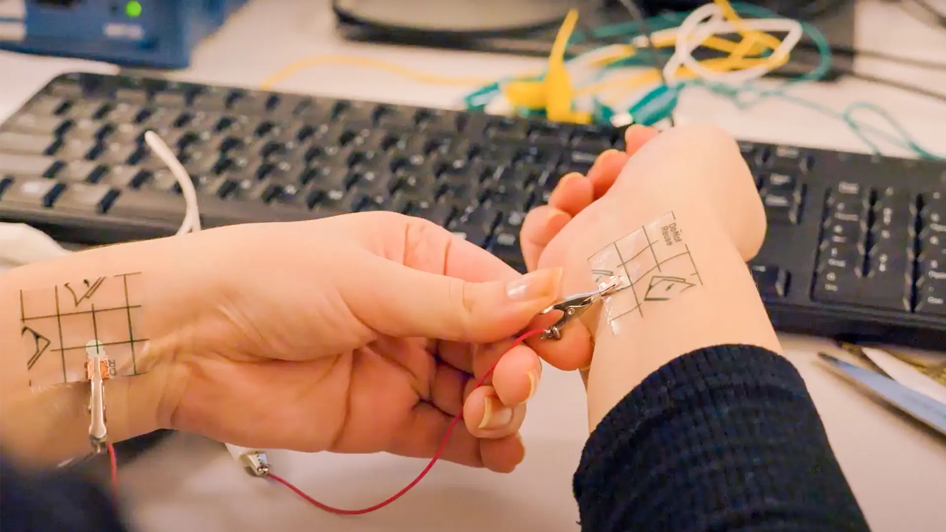
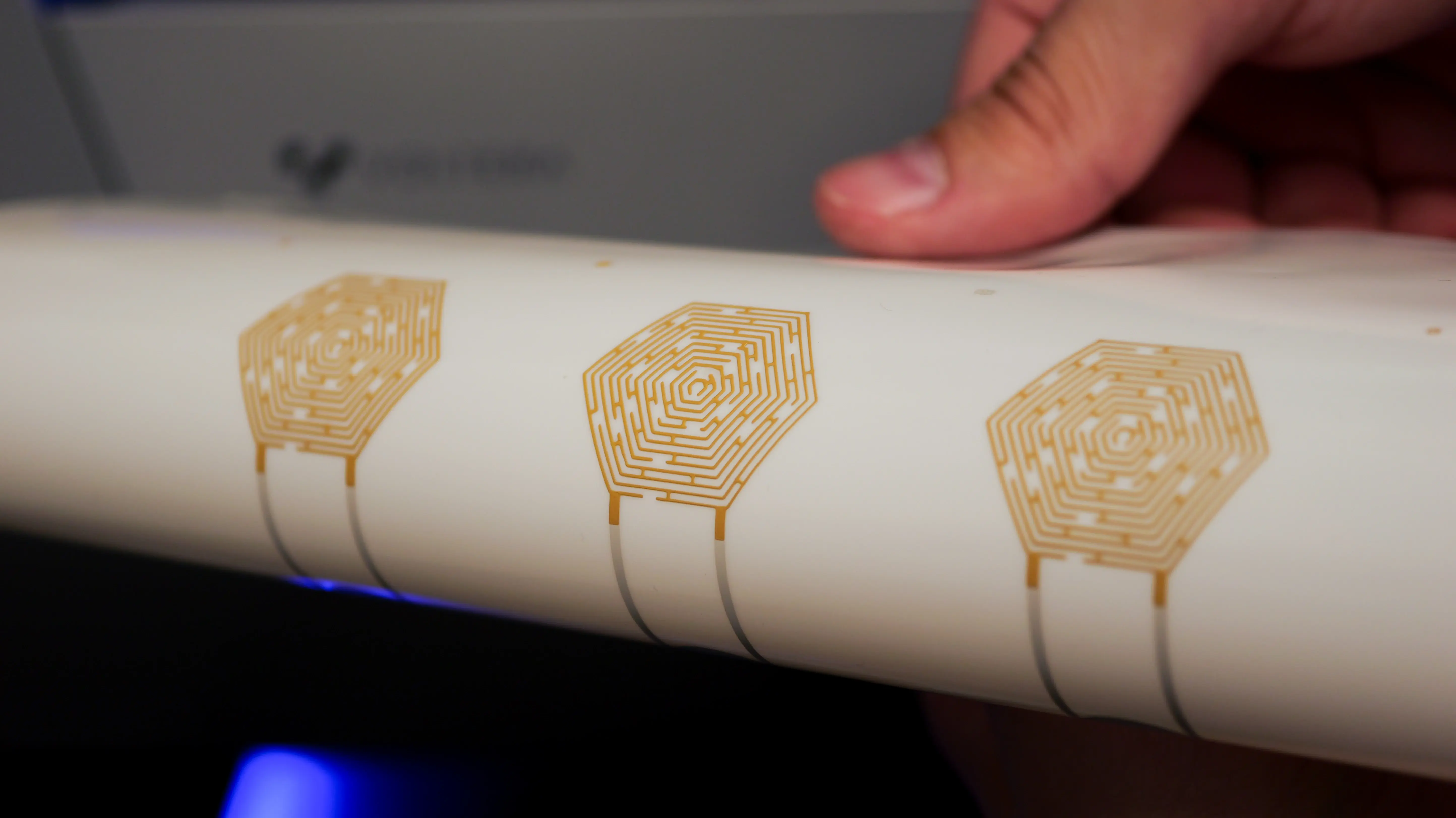
In practice, DIW systems excel in prototyping wearables, printed sensors, soft robotics, organ-on-chip devices, and other flexible hybrid electronics [2]. These applications benefit from thicker, robust layers with larger amounts of functional material per footprint area [3] compared to inkjet.
For example, a review [1] demonstrated the use of DIW technology in printing:
- Soft sensors with stable and repeatable performance, such as glove-type strain sensors with 10 integrated gauges, fabricated in under 15 minutes
- High-resolution pressure sensors (100 μm features, 0.3 kPa⁻¹ sensitivity, 0-500 kPa range) by tuning rheology for 50 μm nozzles
- Wearable optical and mechanochromic devices, including photonic hydrogel-based strain sensors with reversible color changes under strain
- Fully 3D-printed optoelectronic and electronic components, such as QDLEDs, organic electrochemical transistors, and triboelectric nanogenerators, showing high transconductance, low operating voltage, and robustness
- Printed antennas and gas sensors with porous metal microparticle arrays and tunable resonant frequencies for wireless and environmental sensing.
Outside of academia, industry innovators like Voltera, have also been printing additive electronics and validating new materials:
When to choose inkjet
Inkjet printing is the preferred option when:
- Conductivity and layer thickness requirements are modest, such as low-power, low-speed radio frequency identification (RFID) tags or disposable sensors
- Ultra-fine feature resolution (<50 μm), such as for printed thin-film transistors, antenna arrays, or fine sensors
- Low-viscosity materials are required, such as organic semiconductors or aqueous nanoparticle inks
- Low volume R&D projects where production scalability is not a concern
In summary, inkjet is ideal when you need high-resolution patterning with low-viscosity inks and material economy in early-stage prototyping, especially where manufacturability, solderability, and mechanical durability are not the immediate concern.
Conclusion
Choosing the right approach comes down to whether you're optimizing for device performance and manufacturability (DIW) or fine-scale, low-power innovation (inkjet). Each method plays a distinct role in the broader landscape of printed electronics.
Interested to learn more about technologies for printed electronics and how to choose the best technology that suits your applications? Check out the following resources:
- Printed Electronics: What is Inkjet Printing?
- Introduction to Direct Ink Writing (DIW) Printing Technology
- Introduction to Screen Printing
Want to discuss how our DIW solutions, NOVA and V-One can help with your printed electronics application? Book a meeting with one of our technical specialists.
References
[1] Hou, Z., Lu, H., Li, Y., Yang, L., & Gao, Y. (2021). Direct Ink Writing of Materials for Electronics-Related Applications: A Mini Review. Frontiers in Materials, 8. https://doi.org/10.3389/fmats.2021.647229.
[2] Hossein Baniasadi, Roozbeh Abidnejad, Fazeli, M., Juha Lipponen, Niskanen, J., Eero Kontturi, Jukka Seppälä, & Rojas, O. J. (2024). Innovations in hydrogel-based manufacturing: A comprehensive review of direct ink writing technique for biomedical applications. Advances in Colloid and Interface Science, 324, 103095–103095. https://doi.org/10.1016/j.cis.2024.103095.
[3] Tagliaferri, S., Panagiotopoulos, A., & Mattevi, C. (2020). Direct ink writing of energy materials. Materials Advances. https://doi.org/10.1039/d0ma00753f.

Check out our Customer Stories
Take a closer look at what our customers are doing in the industry.