Webinar Recap: Printing Flexible Electronics on Nanofiber
In this webinar, we invited Dr. Andrew Finkle, Director of NanoPaper™ at Tangho Green Canada, to talk about printing flexible, sustainable electronics using cellulose nanofiber film with Tom Pol, Product Manager at Voltera. The discussion covered how NanoPaper compares to traditional flexible substrates, why substrate choice matters in printed electronics prototyping, and how Voltera’s NOVA materials dispensing system supports process development on novel materials.
Webinar highlights
NOVA for green electronics
The webinar began with a market snapshot of green electronics manufacturing. Tom explained that demand for sustainable electronics is being driven by rising concern around e-waste, increasing regulatory pressure, consumer demand for more sustainable products, and growing interest in circular design and recovery systems. At the same time, adoption is not simple. Sustainable materials still need to balance environmental benefits with durability, scalability, cost, process compatibility, and end-of-life requirements.
Tom then introduced NOVA, Voltera’s materials dispensing system for direct ink writing. NOVA supports high precision dispensing of pastes and is compatible with a broad range of screen printable materials. He highlighted several features that make NOVA useful for prototyping on flexible and novel substrates, including pressure monitoring, surface probing for consistent print height, camera assisted alignment, dedicated multilayer workflow, and a vacuum bed for holding down flexible substrates such as PET, TPU, and NanoPaper.
About NanoPaper
Dr. Finkle then introduced NanoPaper, Tangho Green Canada’s cellulose nanofiber film substrate for printed and flexible electronics. NanoPaper is not intended to replace every flexible substrate. Instead, it gives engineering teams another option when PET or PEN starts to narrow the process window and polyimide feels overengineered for the application.
The material starts with agricultural fiber, which is processed into nanocellulose and formed into a dense cellulose nanofiber film. Unlike conventional paper, NanoPaper has a smoother printable surface and enough mechanical and thermal robustness to support printed electronics workflows.
Many silver ink workflows cure around 120 to 150 °C, where substrates like polyethylene terephthalate (PET) and polyethylene naphthalate (PEN) can often work. However, higher temperature workflows, especially copper ink workflows, can push those materials beyond their limits. Polyimide can handle higher temperatures, but it brings tradeoffs in cost, opacity, and environmental persistence. NanoPaper is positioned in the middle: not as a replacement for polyimide at extreme temperatures, but as a more sustainable and process compatible option when PET or PEN is too limited.
Dr. Finkle also emphasized workflow compatibility. NanoPaper has been explored with screen printing, inkjet, and direct ink writing. For this webinar, the focus was on direct ink writing with NOVA, where silver, copper, and carbon examples have already been printed on NanoPaper. This matters because new materials are more likely to be adopted when they fit into familiar workflows rather than requiring teams to rebuild their process from scratch.
Case studies: Printing on NanoPaper with NOVA
Dr. Finkle shared several NOVA case studies that showed NanoPaper moving from substrate evaluation to functional printed electronics. In one example, capacitive touch sensors were printed on NanoPaper using ACI flexible silver ink, cured at 150 °C for 12 minutes, and shown to sense touch through a polyurethane laminated insulating layer. He also showed additional silver patterns to demonstrate how NOVA and NanoPaper can support rapid iteration across different geometries, line widths, cure profiles, and device layouts.

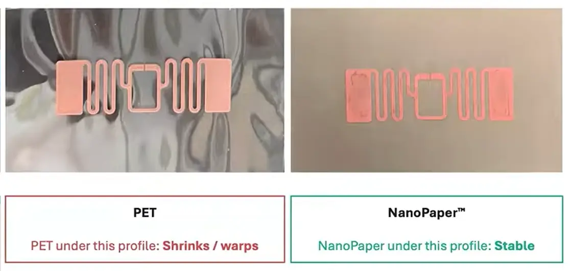
The copper example made the substrate difference especially clear: when the same nanocopper ink, antenna geometry, and cure profile were tested on PET and NanoPaper, the PET substrate shrank and warped under a cure profile around 200 °C, while NanoPaper remained stable. The NanoPaper RFID pattern was then assembled with a commercial RFID module using low temperature solder paste and reflow, then confirmed functional, showing that the substrate could support printing, thermal curing, component attachment, and functional device testing.
Toward the end of the presentation, Dr. Finkle shared the central takeaway: sustainable electronics cannot be only a material story. They also have to be a process story. If a substrate does not fit the way engineers actually print, cure, assemble, and test devices, it will not be adopted. NanoPaper is Tangho Green Canada’s attempt to make renewable cellulose-based films practical inside existing printed electronics workflows.
Live Q&A
Q: What applications are the best near-term fit for NanoPaper?
A: Dr. Finkle highlighted antennas, tags, and sensors as early areas of focus, especially when thermal limits matter. Other potential applications include smart labels, touch interfaces, smart packaging, sustainable single-use circuits, traceability systems, and interactive packaging functions such as food temperature monitoring or tracking high value products.
Q: Is NanoPaper washable?
A: Not likely. Because NanoPaper is cellulose-based, it has an affinity for moisture. The material can be submerged in water and hold its shape, but when it dries again, it becomes much more wrinkled. For that reason, it is better suited to printing-based processes than applications that require repeated washing.
Q: How do you prevent moisture absorption from affecting dielectric properties?
A: Moisture is a repeatability variable for NanoPaper. Cellulose is hydrophilic, so water absorption can affect flatness, curl, dimensional stability, and dielectric properties. The material is durable across many useful humidity ranges, but very humid or wet environments may not be the best fit. As with temperature history for PET, understanding the moisture history of NanoPaper is important for consistent results.
Q: Does NanoPaper hold as well as PET on NOVA’s vacuum bed?
A: Yes. Dr. Finkle said that, in their experience, NanoPaper holds well on NOVA’s vacuum bed. Although the material can absorb moisture at the surface, its dense nanostructure limits moisture and oxygen transmission through the film, helping it form a tight seal. Tom added that in his own experience, the thinner NanoPaper samples held down extremely well on NOVA’s vacuum bed.
Q: What was the initial breakthrough moment behind optimizing a paper substrate for printed electronics?
A: The idea grew from seeing nanocellulose films discussed in literature as potential flexible electronics substrates, but with limited commercial availability. Conventional paper is attractive for environmental and cost reasons, but it has limitations such as high surface roughness and the need for coatings. NanoPaper offered a way to simplify the material stack while improving surface smoothness, thermal performance, and sustainability.
Additional resources
Want to learn more about printing green electronics on sustainable substrates? Check out these resources:
- Video: Printing PCBs on Biodegradable Substrates for End-of-Life Recovery
- White paper: Printing an RFID Tag with Copper Ink on Paper
- Blog: Prototyping Green Electronics with Soluboard® PCB Laminate
Ready to talk about your project? Book a meeting to speak with one of our technical representatives.
Check out our Customer Stories
Take a closer look at what our customers are doing in the industry.