Prototyping Green Electronics with Soluboard® PCB Laminate
Electronic waste, or e-waste, is generated when electronic equipment is discarded. It is estimated that e-waste accounts for about 5% of municipal solid waste across the world. In addition, developing markets are expected to triple their e-waste output in the next five years. E-waste places increasing pressure on waste management systems, and many electronic components contain toxic substances such as mercury, lead, cadmium, beryllium, and arsenic, making them unsuitable for landfill disposal.
At the same time, as risks associated with the global supply chain for rare earth elements and other critical metals continue to evolve, there is growing interest among product developers worldwide in preserving and recovering valuable materials. As a result, innovators have begun exploring ways to recover precious metals and reduce the overall carbon footprint of the electronics industry.
Jiva Materials, a U.K.-based company developing biodegradable PCB laminates, is one of the innovators spearheading such initiatives. Their Soluboard® is the world’s first fully recyclable PCB substrate, with 68% lower carbon footprint than the typical glass fiber and epoxy-based materials. To further explore their innovation, we spoke with Jack Herring, Chief Product Officer and Founder of Jiva Materials.
About Jiva Materials
Q: Can you briefly introduce Jiva Materials and its mission in the field of sustainable electronics?
A: Jiva Materials is an advanced materials company developing Soluboard®, a new generation of PCB laminate designed to reduce the environmental impact of electronics at scale. Our mission is to deliver greener electronics from the ground up — replacing traditional glass fiber and epoxy substrates with a lower carbon alternative that integrates directly into existing manufacturing. By combining naturally derived fibers with a thermoplastic system, we enable a step-change in sustainability without requiring redesign or retooling.
Benefits of Jiva Materials’ Soluboard®
Q: What makes the Soluboard® unique?
A: Soluboard® is engineered specifically for electronics, offering all the performance expected of a rigid PCB — without the glass. It uses a thermoplastic matrix reinforced with natural fibers, enabling a dry lamination process with no epoxy curing stages and significantly lower energy consumption.
The 68% reduction in carbon footprint is achieved not only through the use of cellulosic fibers, but also through this fundamentally lower-energy manufacturing approach compared to traditional glass fiber and epoxy systems. The material is also 37% lower in density than FR4 and remains fully compatible with standard PCB fabrication processes, including plated through-hole technology (PTH).
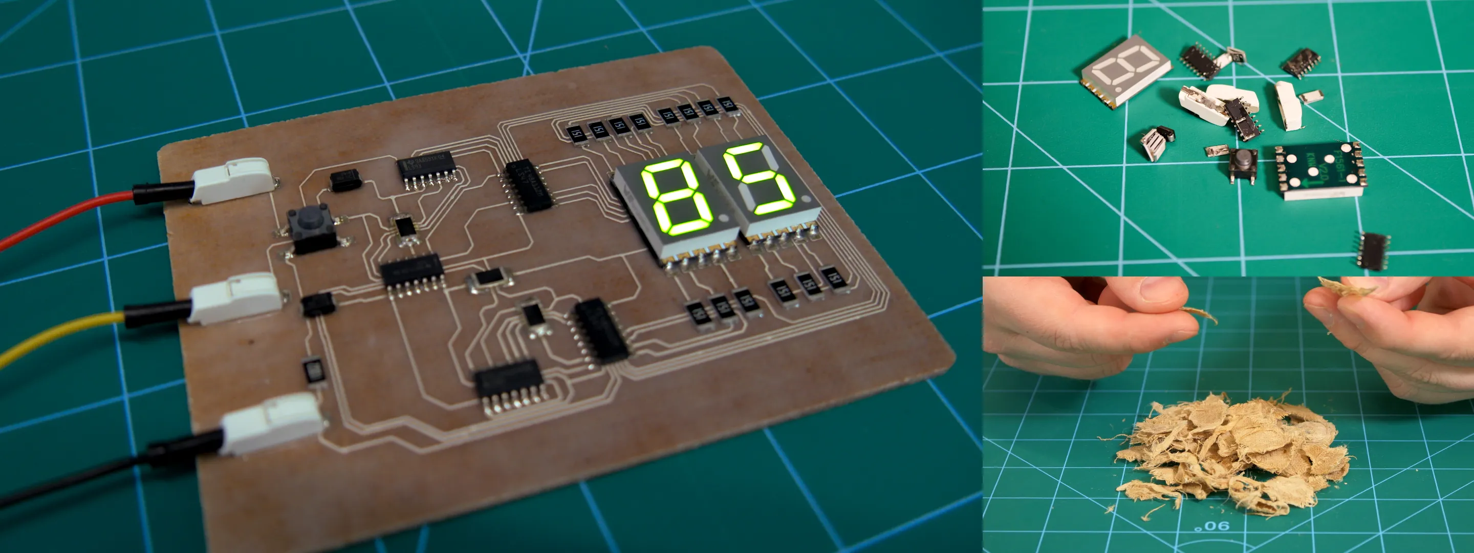
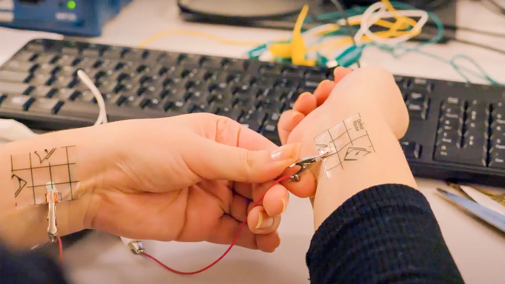
In addition, Soluboard® enables a practical end-of-life pathway. Components can be removed and reused for prototyping or recovery at both lab and commercial scales. Through agitation in hot water, the substrate separates into fibers and a wastewater stream containing the biodegradable polymer and non-brominated flame retardant, which has been independently certified as non-hazardous. The recovered fibers can be mechanically separated and either repurposed or composted, breaking down in approximately 75 days in a natural environment.
Q: What are some benefits of using Soluboard® for green electronics prototyping?
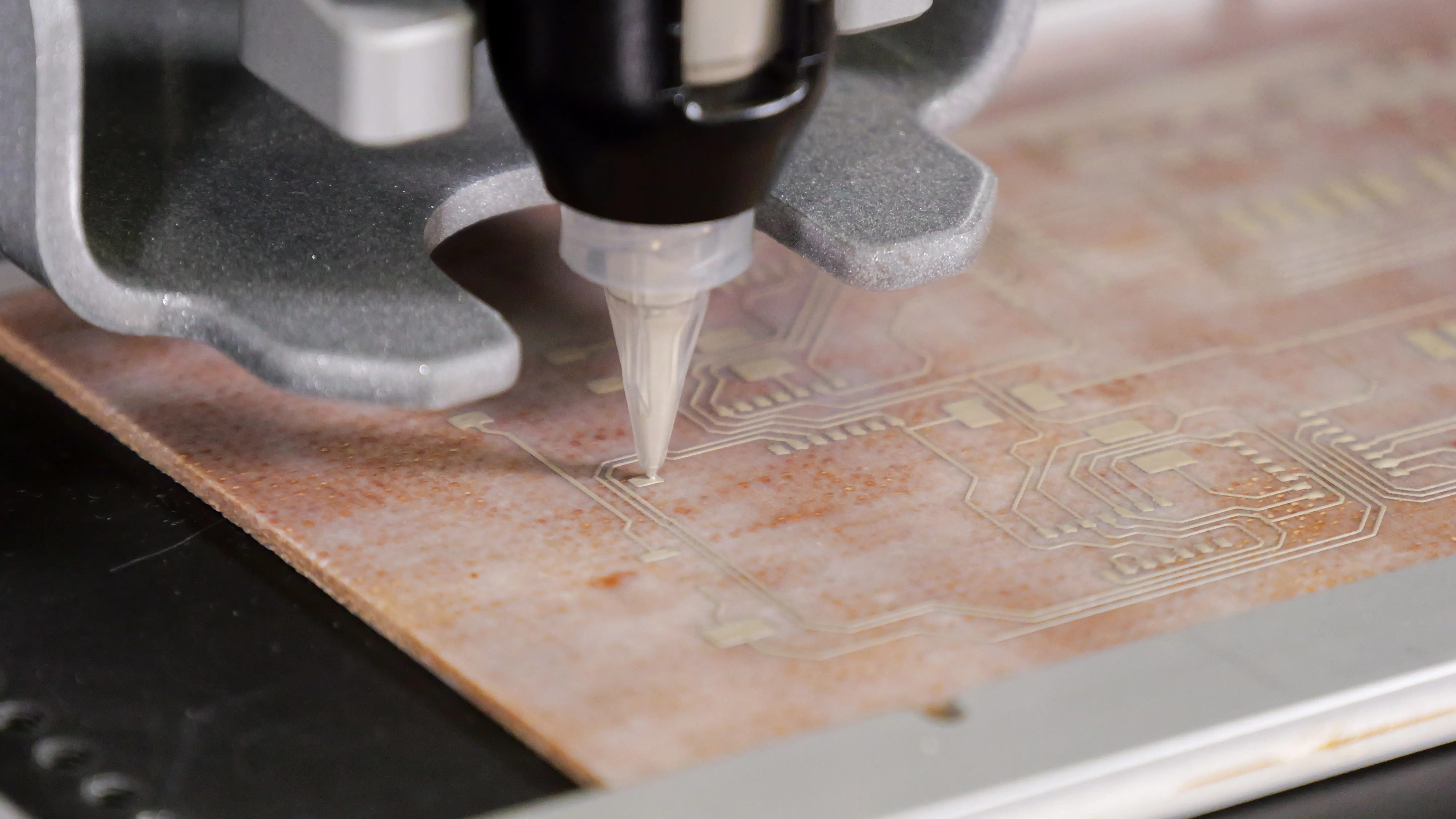
A: Soluboard® allows sustainability to be embedded from the outset without compromising usability. It is easy to machine and handle in lab environments and supports rapid, iterative processes such as screen printing and additive deposition.
Its compatibility with low-temperature processing also reduces energy consumption during assembly. Crucially, it provides a direct pathway from concept to scalable design, allowing teams to develop with a production-ready material rather than switching substrates later in the process.
Scaling from prototyping to production with Soluboard®
Q: How does Soluboard® address its compatibility with sustainable inks and pastes used in direct ink writing and screen printing?
A: Soluboard® has been developed to work effectively with additive electronics processes. We have evolved the fiber system from larger bundles used in early jute-based materials, through flax, and now to lyocell fibers. These fibers are comparable in scale to those used in conventional glass fiber laminates, resulting in a significantly improved surface finish.
This enables reliable wetting and adhesion of conductive inks and pastes, supporting fine feature resolution and repeatable printing in both direct ink writing and screen printing applications.
Q: How well does Soluboard® scale from prototyping to mass manufacturing using screen printing?
A: One of the key advantages of Soluboard® is how effectively it scales. The transition to lyocell fibers has improved material uniformity and continuity, supporting more consistent processing at higher volumes.
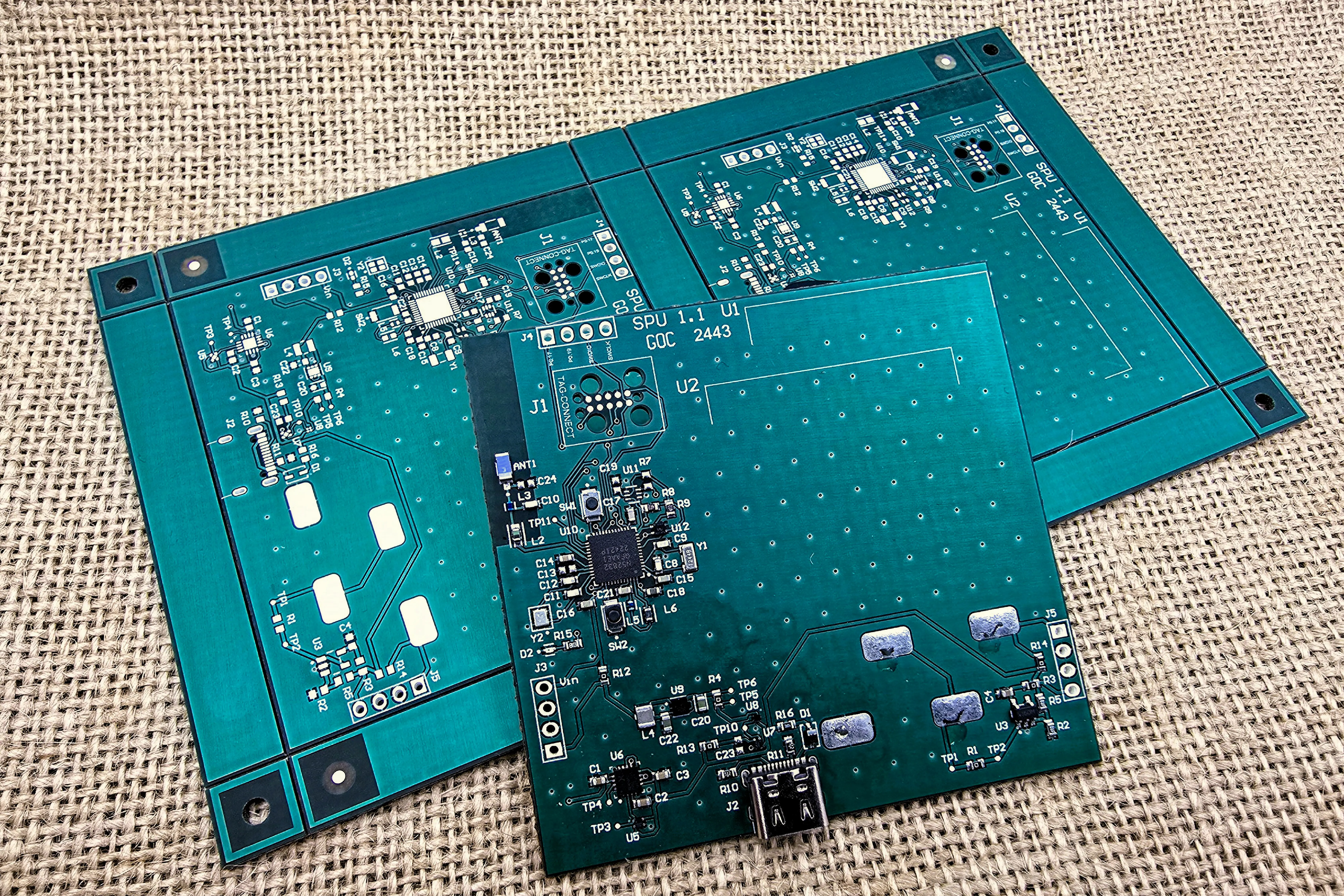
Screen printing, as a scalable production method, has already been successfully demonstrated on the material, enabling a clear route from prototyping to manufacturing. In addition, Soluboard® is available as a copper-clad laminate (CCL), allowing it to be used in conventional subtractive PCB manufacturing where required. This flexibility ensures it can support both additive and traditional production routes depending on the application.
A strong example is our collaboration with Logitech. After being selected as a winner of the Future Positive Challenge, we initially supplied non-copper-clad Soluboard® for prototyping. This enabled exploration of additive and printed electronics in a lower carbon format. The work has since progressed into a broader evaluation across multiple information and communication technology (ICT) peripheral applications, demonstrating how the material can move from early-stage prototyping into real product development.
Additional resources
To learn more about Jiva Materials or Soluboard®, you can visit their website, subscribe to their newsletter, or email them at contact@jivamaterials.com. For regular updates, you can also follow them on LinkedIn.
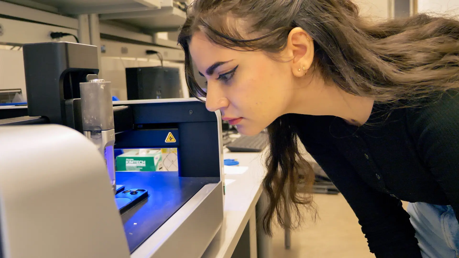
If you’re looking for a prototyping platform compatible with sustainable materials, V-One PCB printer or NOVA materials dispensing system may be a fit. Check out the following projects for more information:
- Video: Printing PCBs on Biodegradable Substrates for End-of-Life Recovery (V-One)
- Video: Printing ECG Electrodes with Biocompatible Gold Ink on TPU (V-One and NOVA)
Ready to talk? Book a meeting to talk to one of our technical specialists.
Check out our Customer Stories
Take a closer look at what our customers are doing in the industry.