Prototyping with Conductive Nano Copper Ink from Copprint
Copprint is an advanced materials company revolutionizing printed electronics with breakthrough conductive copper nanoparticle inks. Founded in 2016, Copprint’s mission is to enable low-cost, high-performance, and sustainable additive manufacturing of conductive components. Copprint’s inks are designed for in-house circuit board manufacturing by replacing chemical etching processes with additive processes.
We recently sat down with Ofer Shochet, co-founder and CEO of Copprint, to talk about prototyping with nano copper inks. Read on to learn what he had to say…
Characteristics of copper nanoparticle ink
Q: What makes copper nanoparticle ink unique from other conductive inks?
Copper ink stands out from other conductive inks due to its:
- Cost-effectiveness: Copper is significantly cheaper than silver and can reduce costs by 5 to 10 times.
- High-conductivity: When properly sintered, copper offers excellent electrical performance.
- Sustainability: Copper has the lowest CO₂e per performance relative to any silver or carbon conductive ink. The carbon footprint of conductive copper inks is 40 times less than silver. Copper’s carbon footprint is also slightly lower than carbon’s, and it delivers the same electrical performance using 100 to 1,000 times less material.
- Abundance: Copper is much more abundant and affordable than silver, ensuring a stable and scalable supply, as well as lower costs and reduced cost volatility.
- Recyclability: Copper inks can be composted and recycled.
Benefits of Copprint ink for rapid prototyping
Q: What are the benefits of using Copprint ink for rapid electronics prototyping?
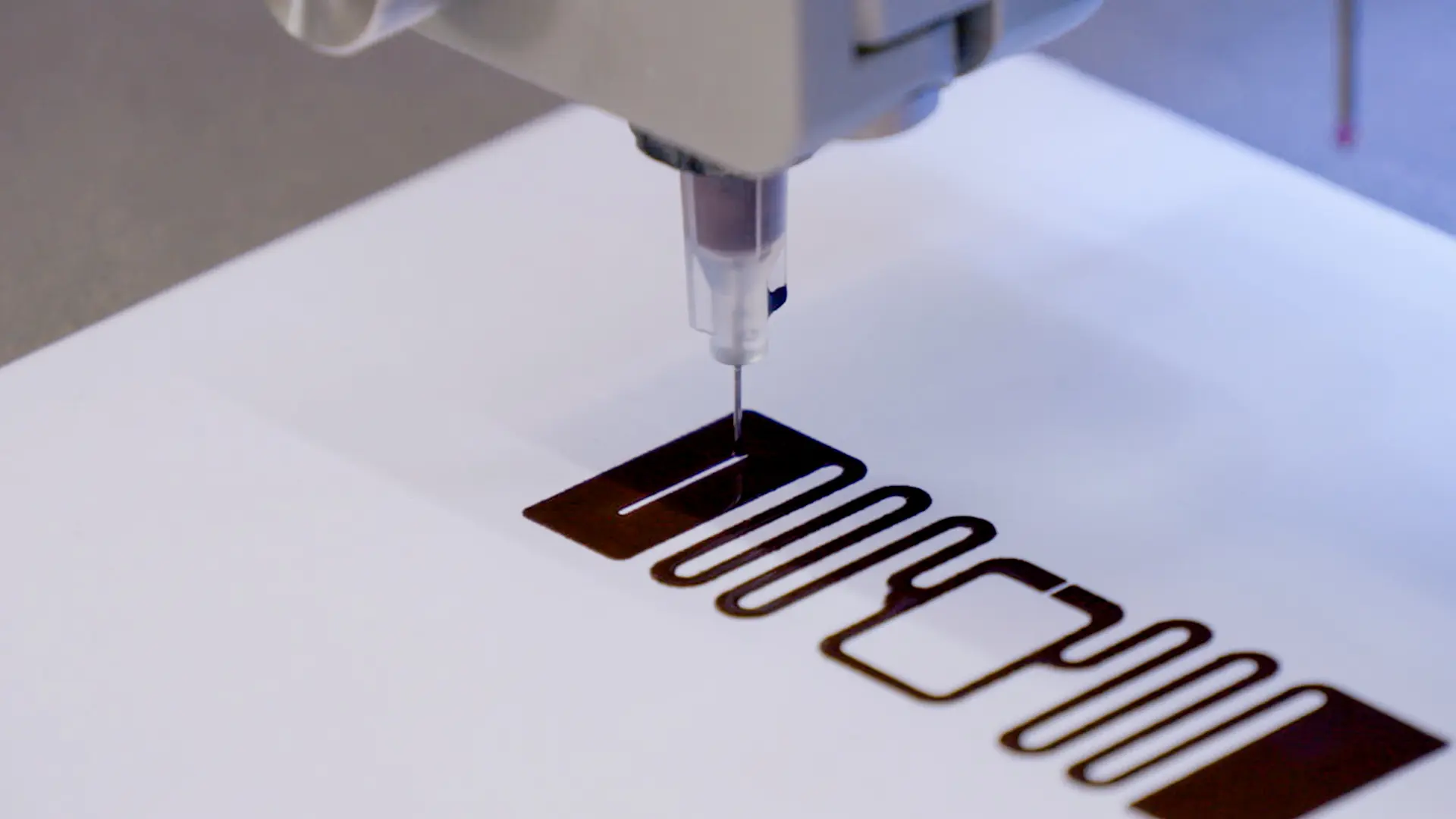
Copprint copper nano inks are designed for speed, precision, and flexibility, making them ideal for rapid prototyping. Their print-ready formulations work with standard printing techniques, allowing engineers to quickly iterate designs without specialized equipment. The conductive inks are sintered in seconds at 150-300°C, depending on the substrate, enabling fast turnaround times and low-cost development for functional prototypes.
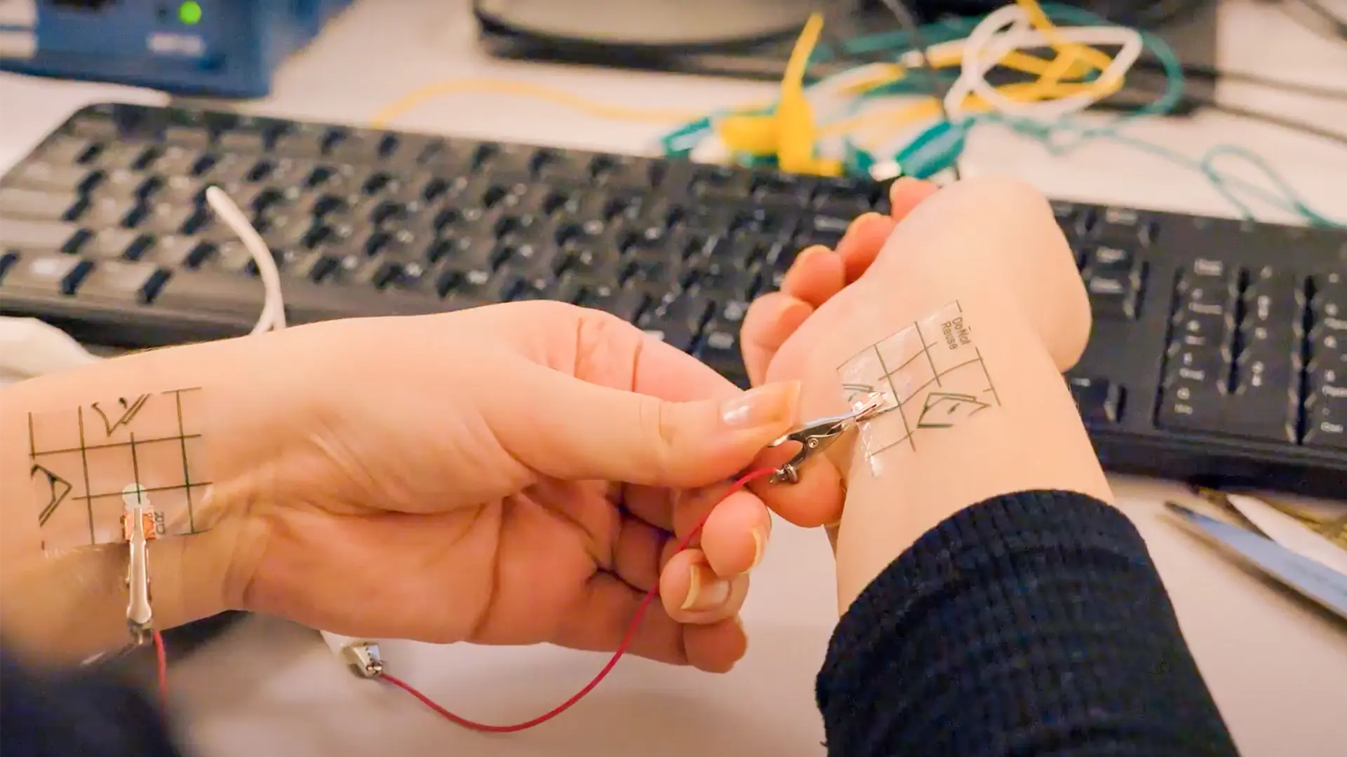
Additionally, the inks support fine geometries and high-resolution patterns, making them suitable for complex circuits in applications like wearables, IoT devices, and smart packaging. Since copper nano ink can be used for both prototyping and large-scale manufacturing, using it during the prototyping phases facilitates a smoother transition to mass production.
Nano copper ink sustainability benefits
Q: What sustainability benefits does nano copper ink offer?
Additive manufacturing with copper conductive inks offers a sustainable alternative to the highly polluting chemical etching processes used in traditional circuit board production. By using nano copper inks in a design-for-additive-manufacturing (DfAM) approach, engineers can print copper only where it’s needed, eliminating the wasteful etching of copper-clad laminates. This method not only reduces material usage and cost but also enables ultra-thin copper layers, lighter boards, and integrated functionality.
Copper inks are also highly recyclable and serve as a more affordable and abundant substitute for expensive and scarce silver used in silver-based inks. Copprint’s additive process further enhances sustainability by cutting CO₂ emissions by over 50% and minimizing the use of water, energy, and toxic chemicals. This approach supports cleaner production and contributes to a smaller environmental footprint and is already being explored in flexible electronics, smart fabrics, and embedded IoT systems.
Rheological requirements for DIW and screen printing
Q: How do your ink formulations address the rheological requirements for compatibility with direct ink writing and screen printing?
Copprint’s inks are engineered with precise rheological control to ensure compatibility with a wide range of additive PCB manufacturing methods. The formulations maintain optimal viscosity, surface tension, and particle dispersion, allowing for smooth flow, accurate deposition, and excellent adhesion. The inks deliver high-resolution patterns with minimal spreading or clogging across both rigid and flexible substrates, supporting scalable production and prototyping.
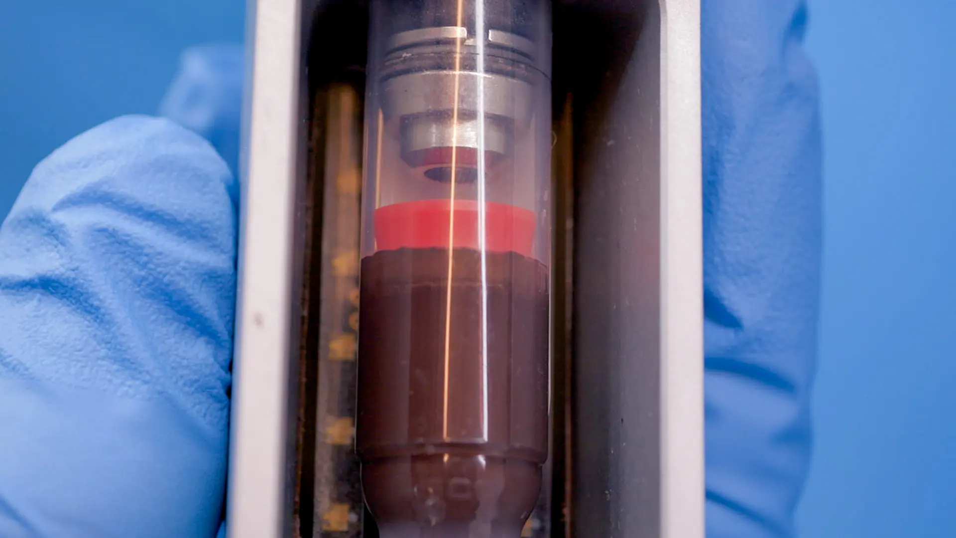
The product portfolio of inks is designed for specific substrates, and the viscosity, thixotropy, and particle size distribution (PSD) are tailored to fit different printing techniques and outcomes such as thin or thick printing.
The entire product portfolio is compatible with the NOVA materials dispensing system.
Copprint ink in innovative prototyping
Q: Can you share an interesting or innovative project that has used Copprint ink in a prototyping context?
An example is the process towards large-scale manufacturing of radio-frequency identification (RFID) antennas. The prototyping phase requires many cycles for optimal radio frequency (RF) design and many different circuits and tests. As optimization needs to be done using the same manufacturing technique, using copper inks for both prototyping and large-scale production makes this possible.
To learn more about Copprint and their copper nanoparticle materials, visit their website or reach out to them at info@copprint.com.
Additional resources

Check out our Customer Stories
Take a closer look at what our customers are doing in the industry.