Webinar Recap: Printing Biodegradable PCBs
In this webinar, our Support Lead, Nathan Shinkar, was joined by Jack Herring, founder of Jiva Materials, to explore how Soluboard®, a biodegradable PCB substrate, offers a sustainable alternative to traditional FR4 boards. The session included insights on sustainability in PCB prototyping, an in-depth look at Soluboard, and how easily it integrates with our V-One PCB printer.
Webinar highlights
Why sustainability matters in PCB prototyping
Nathan kicked off the session with a look at how additive electronics, more specifically direct ink writing (DIW), help reduce e-waste:
- Print only where needed — less material waste
- No harsh chemicals or etching processes
- No need for offshoring or bulk orders — fewer shipping emissions
- Compatible with recyclable and biodegradable substrates like Soluboard®
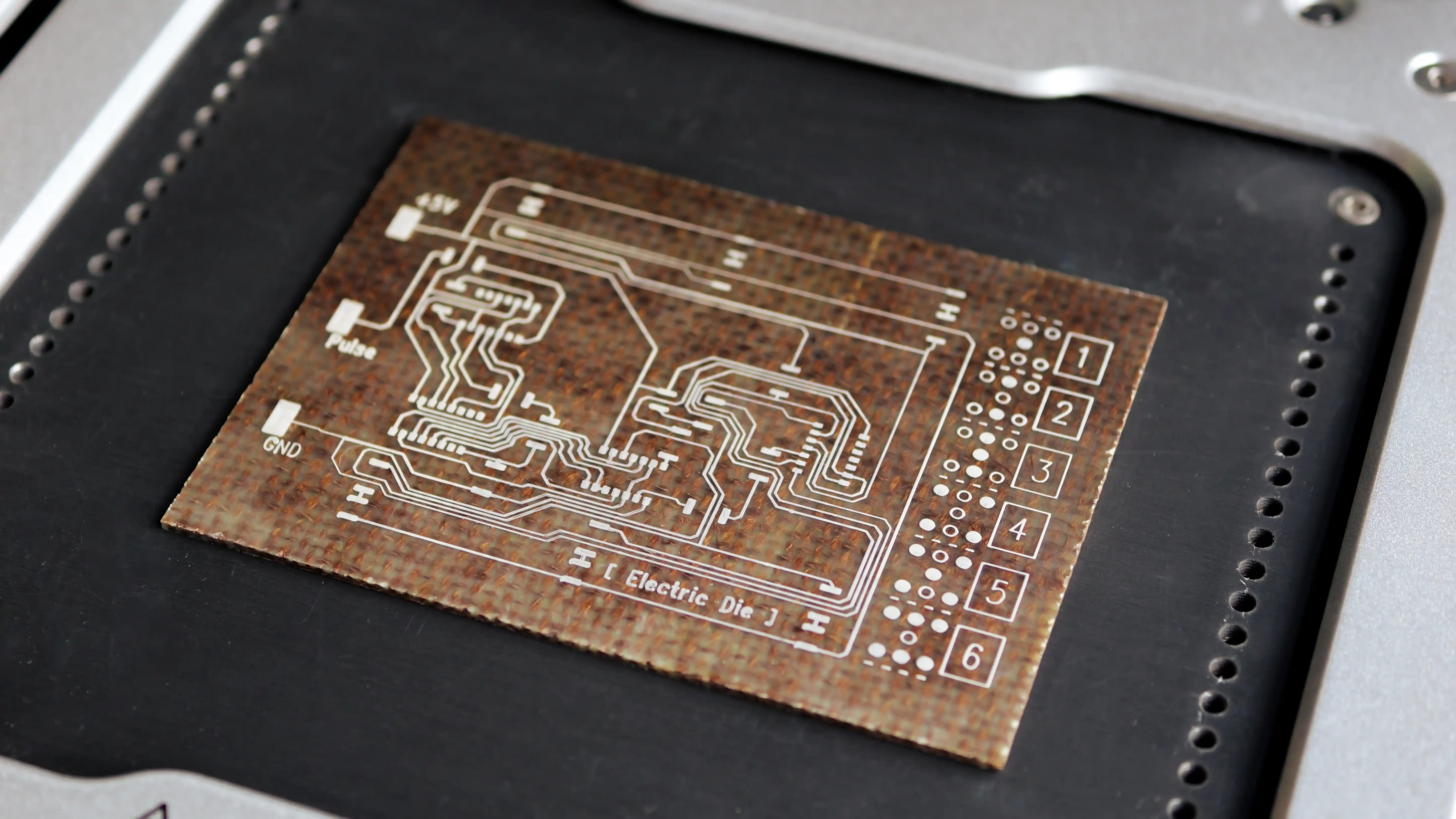
As a DIW PCB printer, V-One supports eco-conscious development by enabling desktop additive PCB prototyping with conductive ink printing, solder paste dispensing, and reflow, all without relying on traditional subtractive manufacturing methods. For more advanced builds, the V-One also offers through-hole drilling to support double-sided circuits.
Soluboard®: The world’s first recyclable PCB substrate
Jack Herring introduced Soluboard, a biodegradable and recyclable thermoplastic laminate made from natural fibers like jute and flax. Compared to FR4, Soluboard:
- Has a reduced carbon footprint of over 68% (up to 73% for thin substrates)
- Supports metal recovery via a non-hazardous hot-water recycling process
- Fully decomposes natural fiber layers in ~75 days post-recycling
- Is UL-recognized and compatible with through-hole and double-sided PCB designs
- Is already used by original equipment manufacturers (OEMs) for sustainability-compliant hardware development
Soluboard performs reliably in environmental and thermal testing, with lower thermal expansion than FR4—minimizing delamination and warping during soldering.

Integrating Soluboard® with V-One
Soluboard integrates directly into the V-One workflow:
- Works with the V-One’s standard bake and reflow steps
- Supports two-sided PCB prototyping with drilling and rivet pressing
- Compatible with Voltera’s low-temp soldering process
Soluboard is now available in limited quantities through the Voltera Store.

Live Q&A
- Q: How long does it take for Soluboard to biodegrade?
- A: ~75 days for natural fibers, after the recycling process.
- Q: Can it support multilayer or buried/blind vias?
- A: Multilayer support is on the roadmap (Q3-Q4 2025). Current minimum via diameter is 0.3 mm.
- Q: Can any PCB shop use Soluboard?
- A: Yes, with coordination through OEMs or direct inquiry to Jiva Materials.
- Q: What polymer is used in the blend?
- A: Polyvinyl alcohol (PVA), chosen for performance and minimal environmental impact. For more information, refer to their patent document.
- Q: Is Soluboard compatible with immersion cooling or flexible PCBs?
- A: Soluboard is not currently designed for immersion-cooled or flex PCBs, but testing is ongoing.
- Q: What are the dielectric properties?
- A: Dielectric constant ranges from ~3.5 to 4, depending on fiber type.
- Q: How thin can the substrate go?
- A: Currently down to 0.3 mm, with thinner variants under development.
Additional resources
Want to learn more about sustainable PCB prototyping and how Voltera’s products help create greener electronics? Check out these resources:
- Blog: Prototyping with Sustainable Conductive Nano Copper Ink
- White paper: Printing PCBs on Biodegradable Substrates for End-of-Life Recovery
- Application: Additive PCB Prototyping
Ready to talk about how V-One can help you make green electronics? Book a meeting to speak with one of our technical representatives.
Check out our Customer Stories
Take a closer look at what our customers are doing in the industry.