How to Design a Printed Circuit Board (PCB)
Just like any type of project, the first step of printed circuit board (PCB) prototyping is ideation, where you define the core functionality and components of your circuit. If PCBs serve as the “brains” behind nearly all electronic systems, then designing the board is like meticulously mapping the brain's neural pathways. You are drawing the intricate arteries and veins that will carry power and signals, enabling the entire system to think and function.
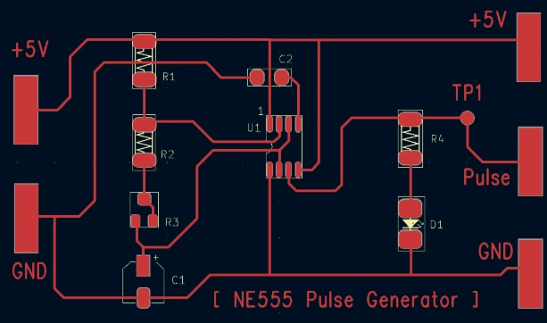
Workflow of designing a PCB
The exact workflow can vary with project needs, but generally it involves defining the project requirements, choosing components, and drawing the schematic. This is followed by setting up component placement and routing the conductive traces in a PCB layout tool.
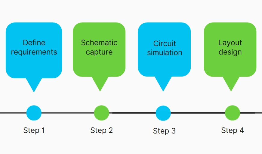
Once the layout is complete, the final steps include running design rule checks (DRC), generating manufacturing files (like Gerbers), and importing the files into a PCB printer’s software, like the V-One software, to prototype the physical board. Alternatively, if you’re outsourcing to a PCB manufacturer, you’ll need to upload the files to their website, communicate your requirements, and wait for the finished boards to be shipped.
Defining project requirements
Every PCB design begins with a clear definition of the project requirements and constraints. At this stage, the goals and specifications of the circuit are determined based on the intended application and environment.
Important considerations include:
- Functionality of the circuit, such as
- Signal processing
- Power delivery
- Microcontroller logic
- Performance metrics that influence component choices and layout (e.g., low-level amplifier circuits have special needs for well-placed microstrip interconnections [1].)
- Environmental constraints, such as
- Size and form factor of the board
- Ambient temperature range
- Expected mechanical stresses
- Any enclosure that the PCB must fit into
- Regulatory standards or certifications like electromagnetic interference (EMI) regulations and safety standards that the design must comply with
- Budget, which can affect component selection and board complexity.
With these requirements, you’ll be able to select specific components for each function. It’s recommended to consult datasheets and supplier catalogs, and you may want to use manufacturer simulation tools to evaluate components.
With clear requirements and a concept in mind, the next step is to design the circuit schematic. Schematic capture means creating a diagram that shows all electronic components and how they are electrically connected with nets according to the circuit logic.
You might have drawn a circuit schematic with a paper and pencil before, but to streamline PCB development, you’ll need to design it digitally with electrical computer-aided design (ECAD) software, or electronic design automation (EDA) software.
Using ECAD software offers numerous advantages:
- Digital files are inherently cleaner and easier to modify than hand-drawn, erased papers.
- All professional ECAD tools include DRC to flag errors like unconnected wires (opens) or incorrectly spaced traces.
- It’s easy to transition from a schematic to a PCB layout within the software.
- Component libraries store component footprints and symbols.
Choosing your ECAD software
There are many EDA software options available. While commercial packages excel in large-team environments and complex design rule management, free or open-source tools like KiCad provide robust capabilities at no cost, which is ideal for individuals or schools on a budget.
Commonly used ECAD software
| Software | Cost | Pros | Cons |
|---|---|---|---|
| KiCad | Open-source (free) |
|
|
| LibrePCB | Open-source (free) |
| |
| Eagle (Autodesk) | Proprietary (free version available) |
|
|
| Altium Designer | Proprietary |
|
|
Best practices for drawing schematics
When drawing a PCB schematic, it is important to indicate all connections clearly, including power rails and ground references. It’s also recommended to organize the schematic logically (grouping related components into sections, using labels for nets) so that it’s easy to review and understand.
At this stage, designers also assign reference designators to components (U1 for the first IC, R1 for the first resistor, etc.) and ensure each component’s symbol is linked to the correct physical footprint.
It also helps to plan ahead for trace widths — especially for power and ground lines, which should be wider to reduce resistance and handle current more safely. Wider traces are also more durable for hand soldering. If unsure, you can estimate appropriate widths with tools like this PCB trace width calculator.
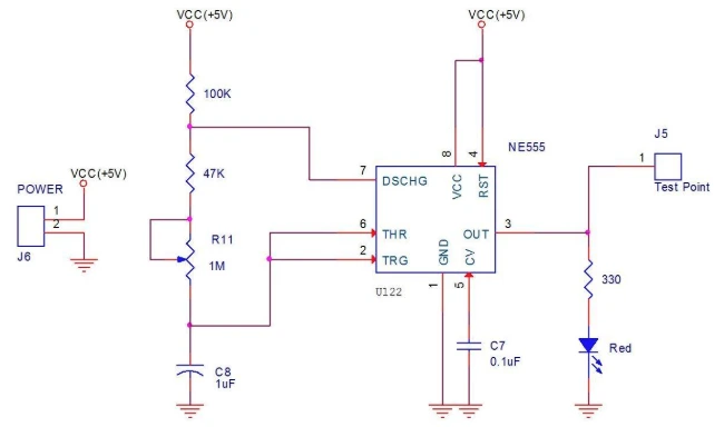
Circuit simulation
Before committing the design to a PCB layout, it’s often beneficial to simulate the circuit or otherwise verify its behavior [1]. Many ECAD tools like KiCad have built-in simulation support, which enables designers to check things like amplifier gains, filter responses, signal integrity, or power supply stability.
PCB layout design
Once the schematic is finalized and verified, the design moves into the PCB layout stage. In general, a completed schematic is transferred to the PCB layout tool, carrying over all components and the netlist. Many ECAD tools like KiCad allow synchronizing or updating the PCB from the schematic, ensuring consistency between them. This is where the abstract schematic is turned into a concrete board design. This involves a few steps:
- Board setup: Based on the earlier requirements and any mechanical constraints, the designer defines the PCB dimensions and layer stackup.
- Component placement: Components are imported into the layout, each represented by a footprint that specifies the pads or holes where the part will be soldered.
- Routing traces: According to the schematic netlist, conductive traces that connect the component pins are drawn, adding through-holes that allow a trace to jump from one layer to another as needed.
Refinement
After completing the layout, designers perform a comprehensive design rule check using the ECAD software. This includes checking that no traces are too close, no copper features violate spacing or size constraints, and there are no unintended overlaps or copper islands. If the DRC finds errors, they should be addressed before exporting the finalized board design for production.
Conclusion
The complete workflow of PCB design incorporates a lot of quality check steps, which are essential for the success of the board. By organizing the process into clear steps and addressing important considerations at each stage, PCB designers can transform an idea on paper into a working PCB without surprises.
Interested in learning more about PCB design? Check out these resources:
- Customer story: Revolutionizing PCB Design Education with V-One
- White paper: Printing a Decimal Counter Circuit with Silver Conductive Ink on FR1
- Blog: Autodesk ❤ Voltera
Want to explore PCB prototyping with V-One? Book a meeting to speak with one of our technical representatives.
References
[1] Scherz, P., & Monk, S. (2016). Practical Electronics for Inventors, Fourth Edition. O’Reilly Online Learning. https://www.oreilly.com/library/view/practical-electronics-for/9781259587559/.

Check out our Customer Stories
Take a closer look at what our customers are doing in the industry.