White paper
Printing Thermoformable Inks on ABS for In-Mold Electronics
Human machine interfaces (HMI) are the touchpoints that let users interact with electronics, from automotive consoles to appliance panels and industrial equipment interfaces. In-mold electronics support HMI by enabling touch functionality to be integrated directly into shaped plastic surfaces.

- Chimet AG 550 EI thermoformable silver paste
- Chimet D 260 EI thermoformable dielectric paste
- Voltera Conductor 3 silver ink (replaced by Conductor 4)
- ACI Materials FS0142 flexible silver ink
- AG 903 EI conductive adhesive ink
- NOVA materials dispensing system
- Mayku Formbox
- Arduino Uno microcontroller
- Nordson EFD 250 µm dispensing tip
- ZIF connectors
- LEDs
- Jumper wires
Project overview
Purpose
The goal of this project was to validate the compatibility of Chimet’s thermoformable materials with thermoformable ABS, provide practical guidance for prototyping in-mold electronics (IME) in-house, and demonstrate the potential of IME for human-machine interface (HMI) applications.
Design
The project consisted of four parts:
- Printing the capacitive touch sensor circuit
- 3D printing the thermoforming buck
- Thermoforming the printed circuit
- Printing the Arduino interface circuit
Desired outcome
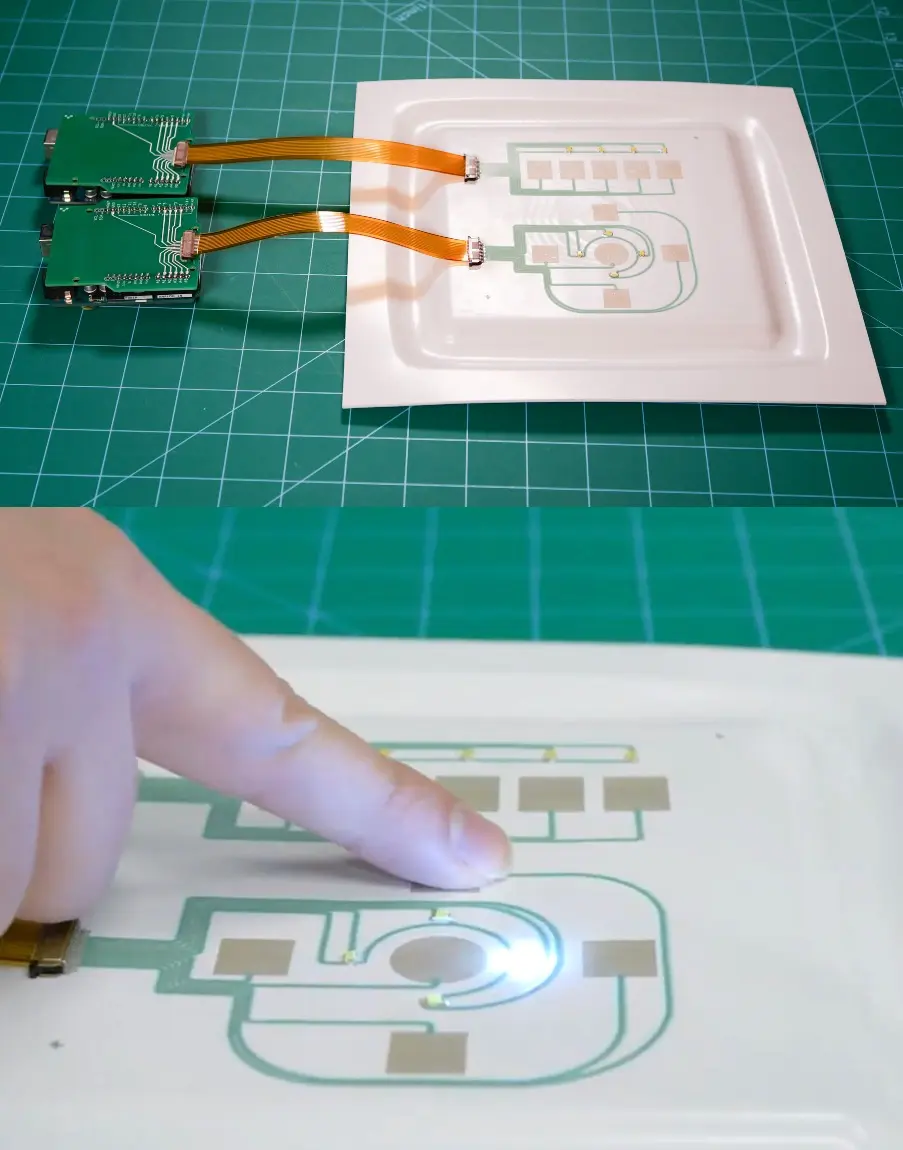
The desired outcome was to develop a capacitive touch circuit that could be thermoformed into a three-dimensional shape without warping, cracking, or losing conductivity. Once populated and connected to the Arduino-based control system, the printed slider and circular control would respond to user input and provide visual feedback through LED activation.
Functionality
Once the sensor was printed, formed, and assembled, we integrated it with an Arduino-based control system to verify real-world operation. The prototype responded to touch input on both the linear slider and the circular control, with LEDs providing immediate visual feedback and confirming successful signal detection after thermoforming.
Printing the capacitive touch sensor circuit
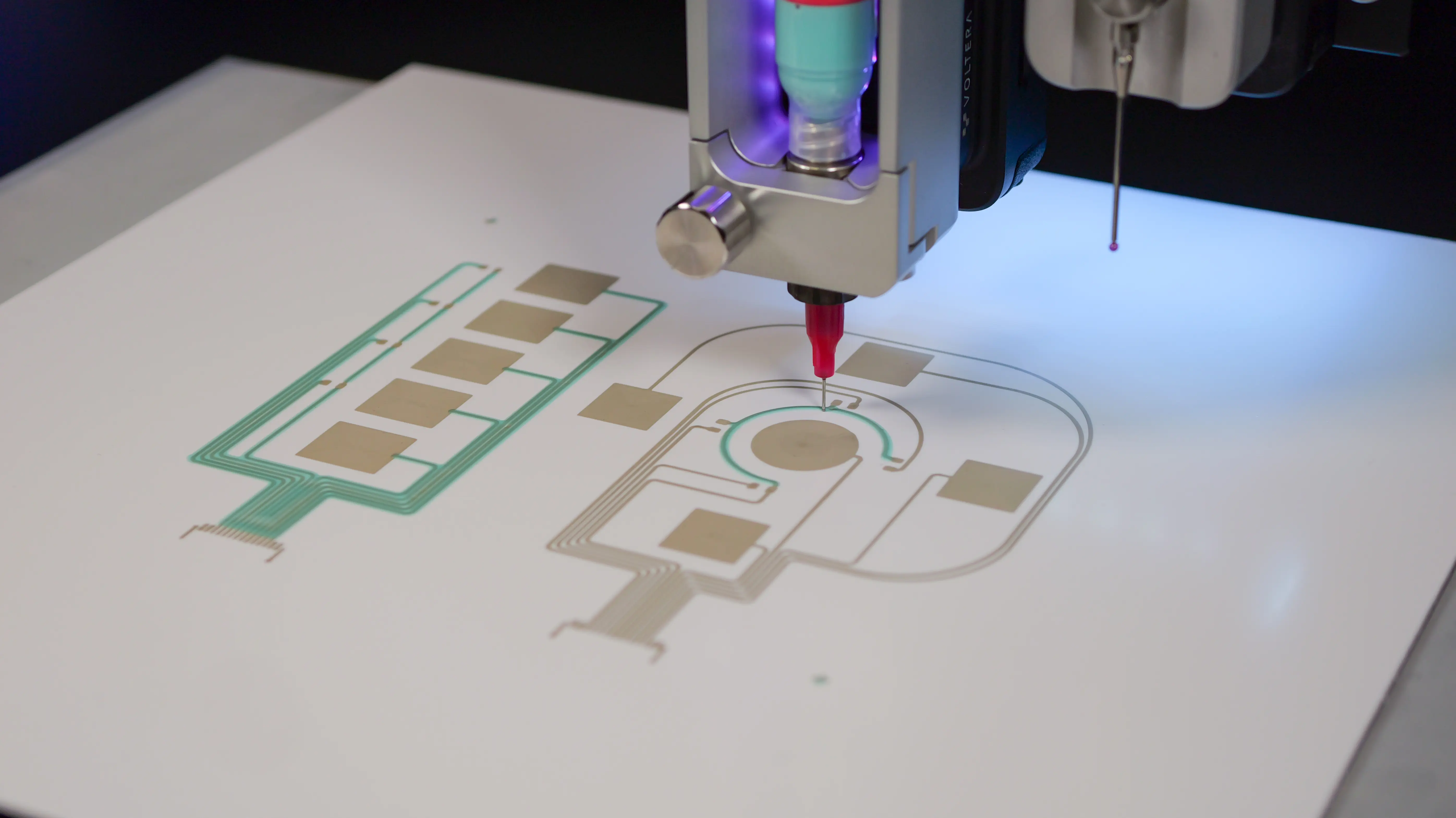
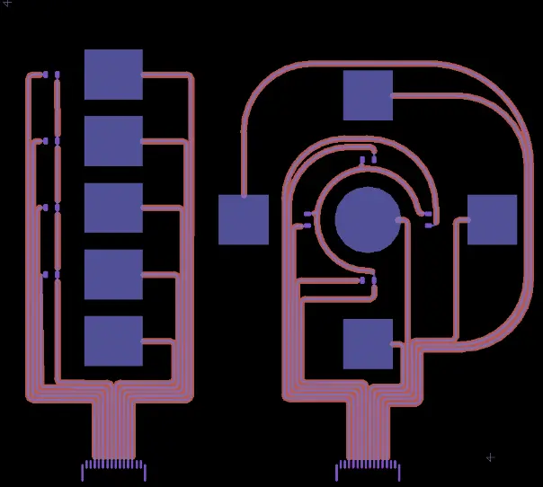
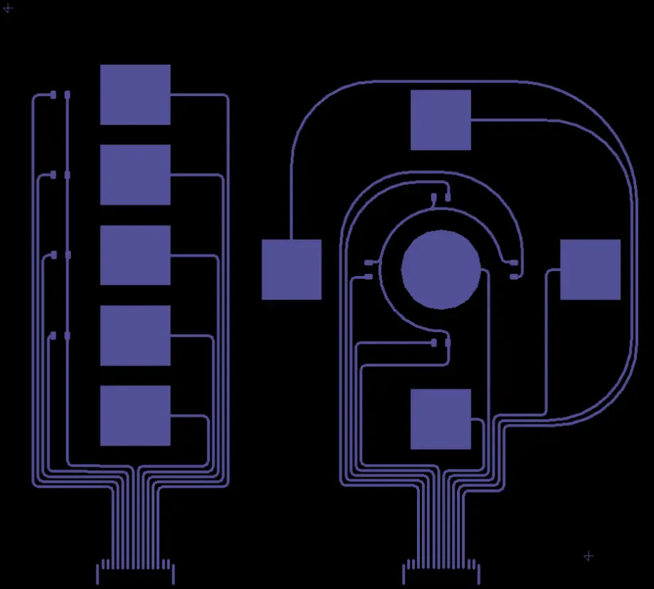
The printed layout included conductive traces, touch electrodes, and larger pad regions for connection and assembly. On top of the conductive layer we printed a dielectric layer to electrically insulate and mechanically reinforce the circuit before thermoforming.
Base conductive layer
The base conductive layer formed the functional circuit geometry, including the capacitive touch electrodes, conductive traces, and connection pads required for later assembly and interfacing.
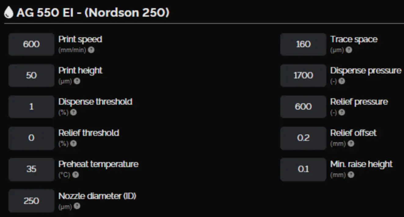
| Paste | Chimet AG 550 EI |
| Substrate | ABS |
| Nozzle | Nordson EFD 250 µm dispensing tip |
| Probe pitch | 5 mm |
| Probe time | 4 minutes and 25 seconds |
| Print time | 33 minutes and 14 seconds |
| Cure time and temperature | 100°C for 20 minutes (ABS has a low softening temperature) |
Top dielectric layer
This layer served two purposes: it electrically insulated the conductive network and mechanically reinforced the printed traces before thermoforming. The added support helped the circuit better resist cracking during the forming step.
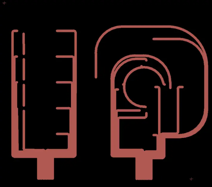
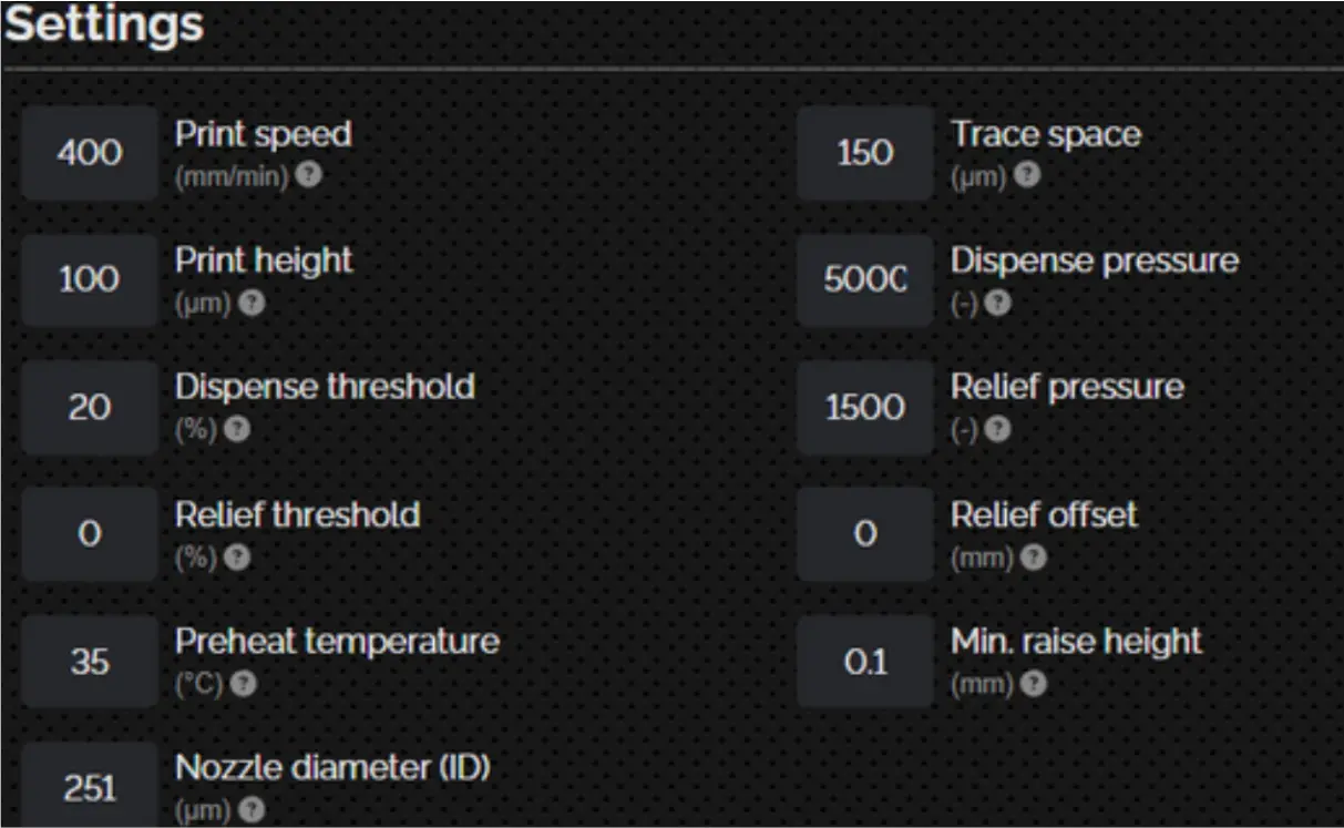
| Paste | Chimet D 260 EI |
| Substrate | ABS |
| Nozzle | Nordson EFD 250 µm dispensing tip |
| Probe pitch | 5 mm |
| Probe time | 3 minutes and 51 seconds |
| Print time | 39 minutes and 55 seconds |
| Cure time and temperature | 100°C for 15 minutes (ABS has a low softening temperature) |
3D printing the thermoforming buck
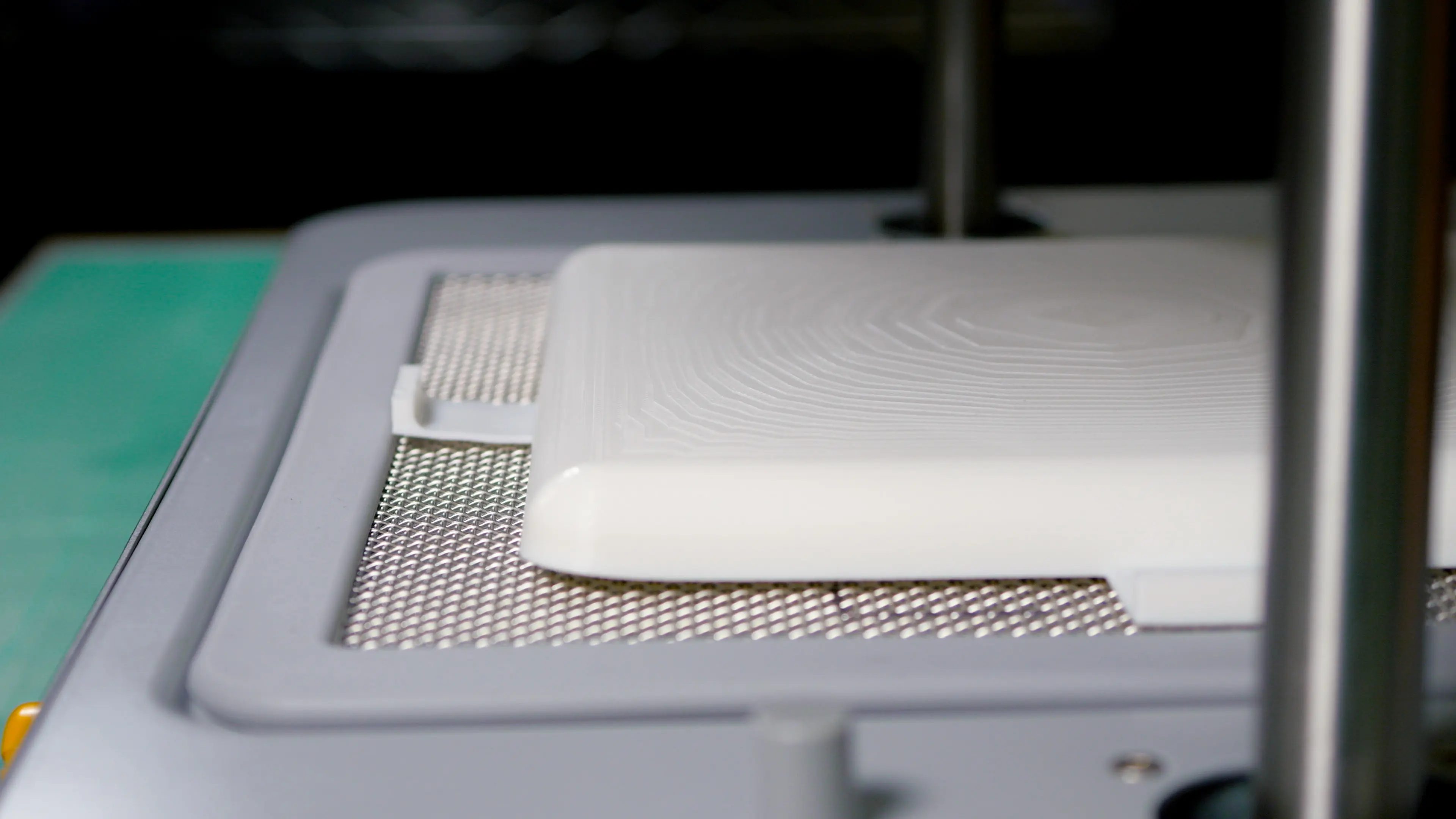
To form the printed circuit into its final three-dimensional shape, we designed and 3D printed a custom thermoforming buck. The buck was developed specifically for this project and incorporated key forming considerations such as draft angle and substrate stretch to help reduce strain on the printed traces and make the formed part easier to remove.
While more complex and dynamic geometries are possible in in-mold electronics, the final buck design was intentionally kept relatively simple to stay within the capabilities of a consumer-grade desktop thermoformer.
Thermoforming the printed circuit
Because this is an in-house project, injection molding was outside the scope, so thermoforming served as the final shaping step. After both printed layers were cured, we thermoformed the circuit using the custom 3D printed buck and the Mayku FormBox for 3 minutes and 30 seconds at heat level 3.5. Once thermoforming was complete, we checked the formed circuit for continuity to confirm that there were no shorts or open connections before moving on to assembly and testing.
Printing the Arduino interface circuit
To demonstrate the capacitive touch functionality of the thermoformed circuit, we also printed a simple Arduino interface circuit on an Arduino Uno shield template PCB (FR4). This board made it easier and more reliable to interface the sensor with the Arduino Uno than using loose jumper wires alone.

| Ink | Voltera Conductor 3 silver ink |
| Substrate | FR4 |
| Nozzle | Nordson EFD 250 µm dispensing tip |
| Probe pitch | 5 mm |
| Probe time | 58 seconds |
| Print time | 2 minutes and 17 seconds |
| Cure time and temperature | 135°C for 15 minutes |
To connect the thermoformed substrate to the Arduino interface circuit, we also printed flexible ribbon cables that connect to the ZIF connectors and route signals from the formed sensor to the interface board.
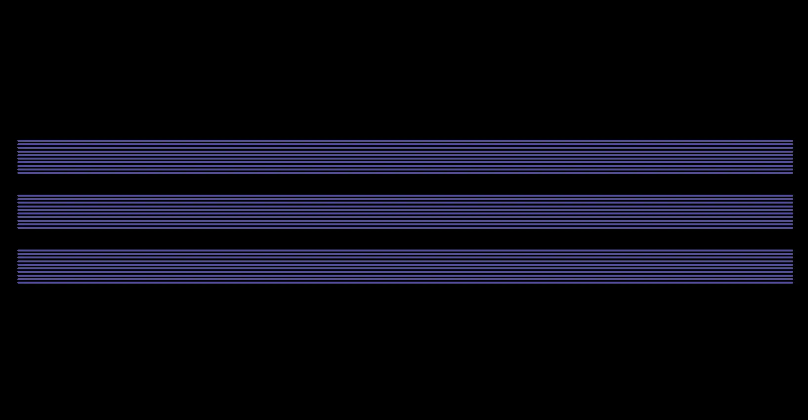
| Ink | FS0142 |
| Substrate | PET |
| Nozzle | Nordson EFD 250 µm dispensing tip |
| Probe pitch | 5 mm |
| Probe time | 3 minutes and 30 seconds |
| Print time | 21 minutes and 31 seconds |
| Cure time and temperature | 150°C for 15 minutes |
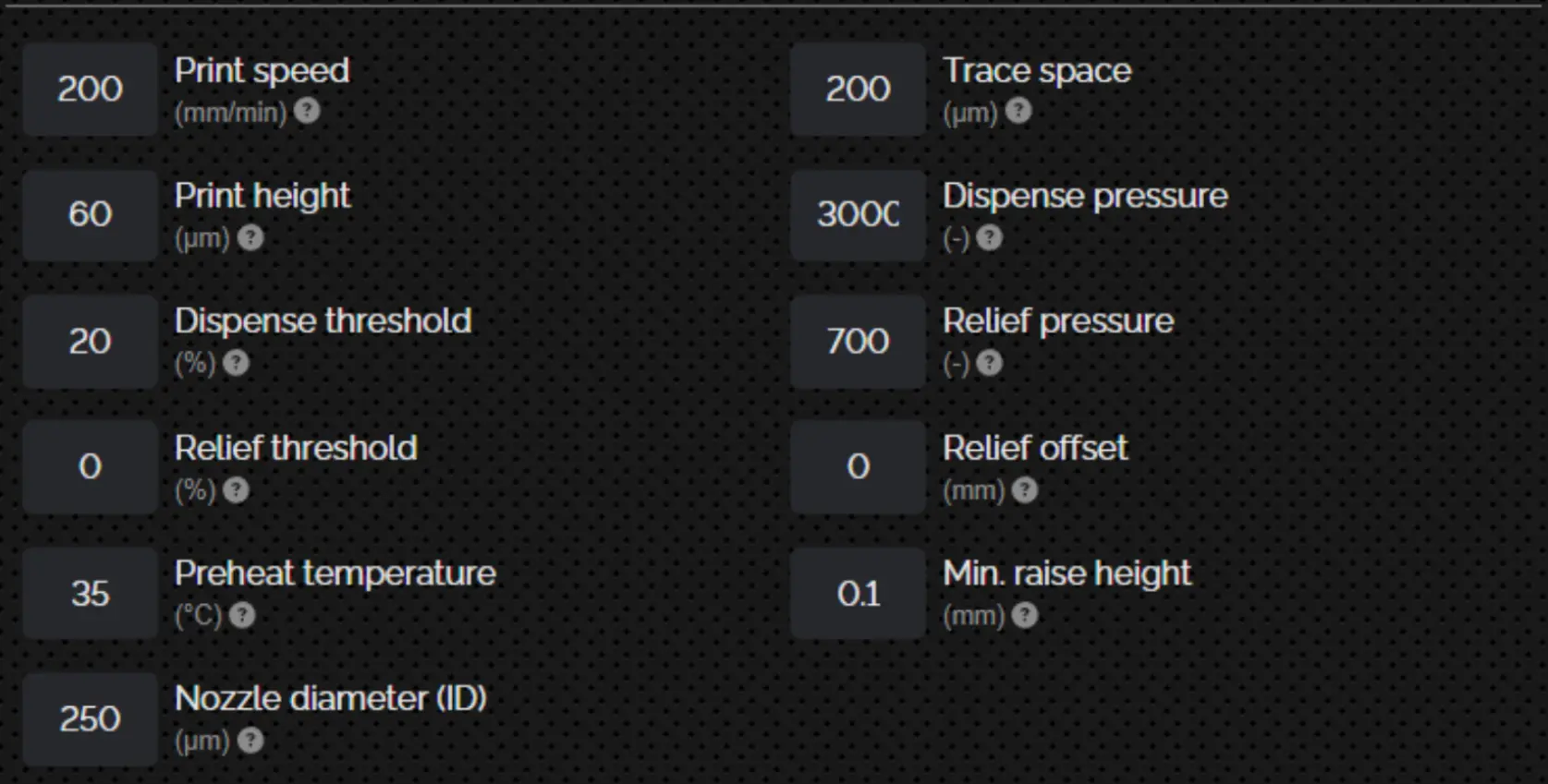
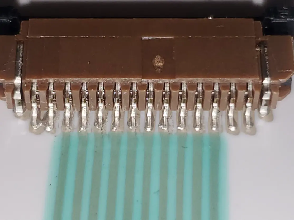
Because standard solder reflow temperatures exceed the softening point of the thermoformed substrate, we manually dispensed Chimet’s conductive adhesive ink, which could cure at a lower temperature, instead of using conventional soldering on the formed part. This helped create an electrically stable and mechanically robust connection between the connector pins and the printed traces without introducing enough heat to warp the substrate.
Challenges and advice
Thermoforming without breaking the circuit
Preserving conductivity through thermoforming required careful process control. Our earlier iterations on PETG and polycarbonate (PC) showed repeated trace cracking after forming, especially in high-strain regions, with fractures on both 1 mm and 0.5 mm PETG after thermoforming, while larger pad regions were less prone to cracking.
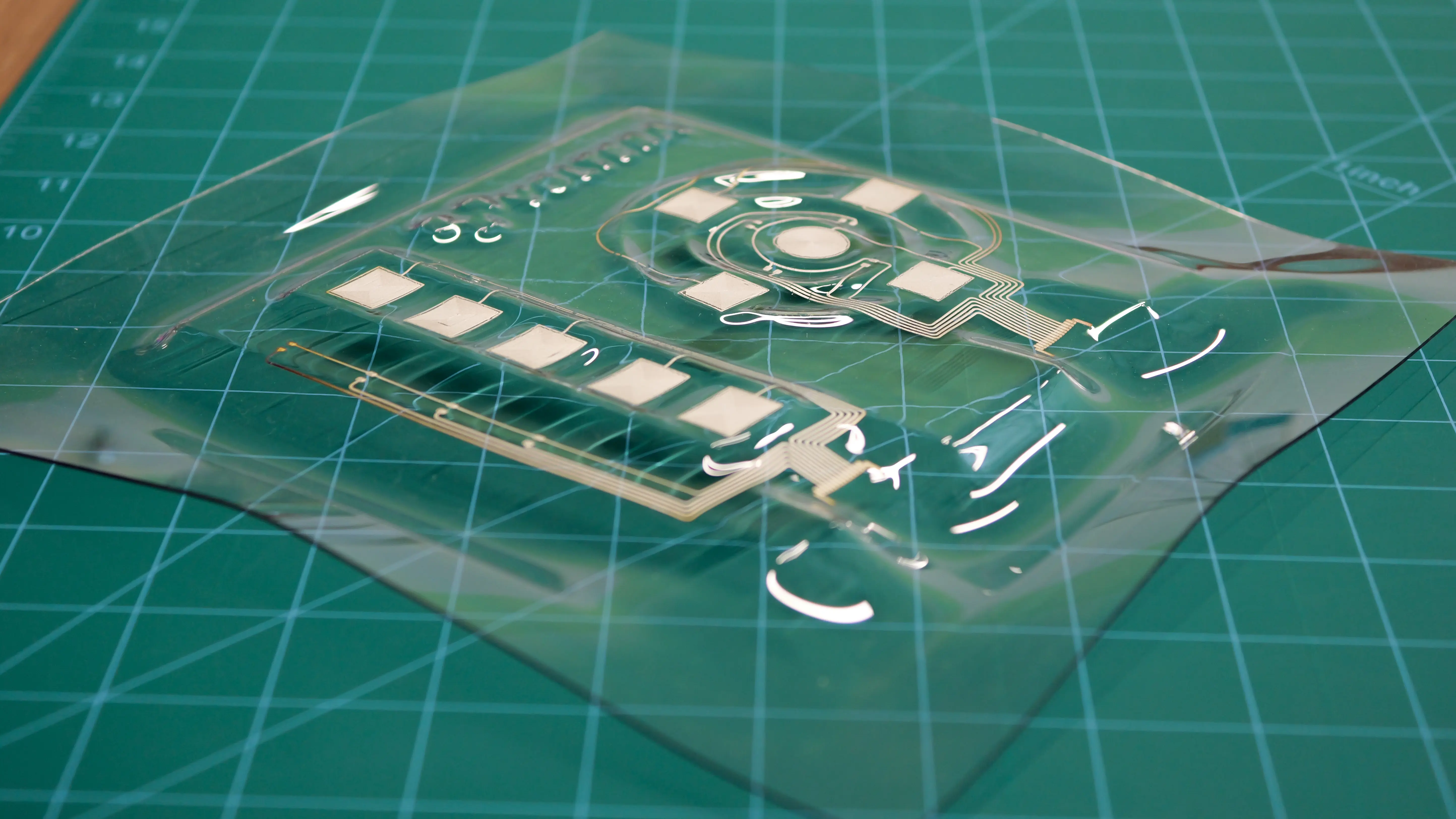
We recommend designing with forming strain in mind from the beginning. Pay close attention to slope, radius, and where the substrate will stretch most. Where possible, reinforce conductive features with a dielectric overprint. It is also helpful to slightly undercure before forming to reduce brittleness.
Material pairing also matters: through trial and error, we shifted from our initial selection of PETG and polycarbonate substrates to ABS. Next, we selected Chimet thermoformable inks which we believed would align well with the substrate and cure windows. It is therefore important to have a materials dispensing system like NOVA readily available so material compatibility can be tested quickly.
Assembly after printing and forming
Our earlier work found that soldering and hot-air reflow could remove pads, flatten formed substrates, or create fragile cable connections. As such, conductive adhesive might be a better fit than solder reflow because it avoids warping or re-softening the part, minimizing thermal stress. We also recommend building strain relief into the connector region. Reinforcement with dielectric, encapsulation, or protective tape can materially improve robustness during handling and testing.
Conclusion
This project demonstrates that in-house prototyping of in-mold capacitive touch interfaces is achievable when material selection, print design, and thermoforming strategy are treated as a single integrated workflow. We hope our process offers product R&D teams a framework for evaluating and iterating future in-mold HMI concepts in-house before moving toward more specialized manufacturing steps such as injection molding.
Using NOVA, we produced a working IME prototype that can be integrated into three-dimensional geometries for HMI. If you’re working on similar projects and would like to discuss materials, tools, and processes, book a meeting with one of our technical specialists.
Frequently asked questions
Could other thermoformable substrates work with this process?
Yes, other thermoformable substrates can work, but compatibility depends on how well the substrate, ink system, and cure window align. With NOVA, you can quickly evaluate how your chosen inks or pastes perform on different substrates, as the system supports a wide range of materials, from flexible, stretchable, and biocompatible substrates to rigid ones.
How do you account for stretching and registration shift during forming?
The main way to account for stretching is to design for the formed geometry from the start, paying close attention to slope, bend radius, and the areas where the substrate will experience the most strain. In practice, this often means iterating both the circuit layout and the thermoforming buck together so the printed features remain aligned and functional after forming.
Could this be integrated behind a cosmetic or protective top layer?
Yes. Capacitive touch does not require direct contact, so the circuit can sit behind a protective layer, which is one reason it is well suited for in-mold electronics and automotive interfaces. In a production IME workflow, the thermoformed circuit would typically be embedded behind an injection-molded surface, such as a car dashboard or control panel.
How durable can in-mold electronics be?
In-mold electronics can be highly durable because they reduce the number of discrete components and eliminate many of the mechanical failure points found in conventional switch-based assemblies. That said, durability depends heavily on material selection, circuit design, strain distribution, and process control, so prototyping and validation are essential before moving toward end-use applications.
Printing multilayer flexible, stretchable, and conformable electronics?
NOVA’s Plan feature makes it easy.