What Is Electronics Encapsulation?
Electronics encapsulation refers to the process of enclosing and protecting electronic components, circuits, or chips in a durable material or “package.” The encapsulating material (sometimes called a molding compound or potting compound) serves as a barrier against environmental factors like moisture, dust, and harsh chemicals, and shields the device from mechanical stress and vibration.
Over the decades, encapsulation approaches have evolved significantly. Historically, hermetic encapsulation (a method of sealing sensitive electronic components inside airtight metal or ceramic enclosures) was common, as it completely blocked moisture and gases. This was especially important in aerospace or military-grade devices [1].
Since the 1970s, the industry has shifted toward polymer-based plastic encapsulation due to its low cost, ease of processing, and high throughput. Today, encapsulating components usually involves applying polymer resins (epoxies, silicones, polyurethanes, etc.) using automated dispensing, molding, or conformal coating systems.
Common types of encapsulation
Potting electronics
In the context of electronics and semiconductors, potting and encapsulation are often used interchangeably. Potting is an encapsulation process where an entire electronic assembly or a larger section of a circuit is placed into a mold (often referred to as a “pot”) and then filled with a potting material (typically a resin) to cure into place.
Potting applications include:
- Submersible or outdoor electronics in harsh environments
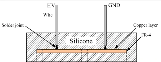
- High-voltage circuits (to prevent arcing) [2]
- Tamper-resistant designs
Dam and fill
A less common variant of potting, dam-and-fill involves first dispensing a high-viscosity “dam” around the component, then flooding the enclosed area with a lower-viscosity encapsulant. Unlike potting, which submerges the entire assembly, dam-and-fill targets only specific areas, allowing precise control over material placement while minimizing resin use. This makes it useful for precision applications or components that require partial exposure, such as optical sensors or fluid-contact electrodes, though it is less widely used than potting or glob-top methods.
Direct encapsulation
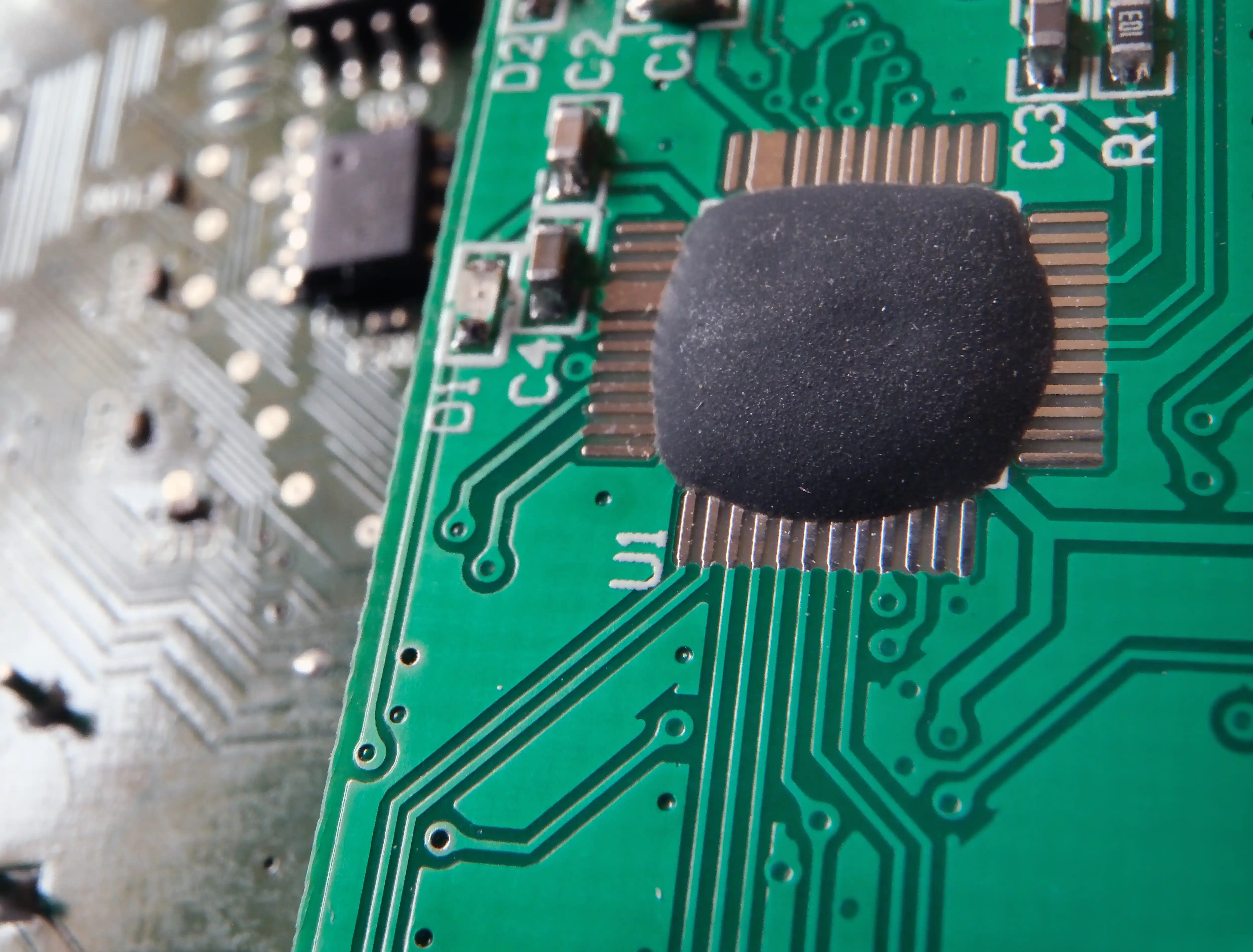
Direct encapsulation refers to dispensing an encapsulation material directly over a semiconductor die or electronic component mounted on a substrate (e.g., a PCB) and then curing it in place. It is a direct method because the encapsulant is applied only to the needed area on the board, without needing a dam or a pot.
Once cured, the dispensed material forms a hardened “glob” that covers the device and its wire bonds. As such, direct encapsulation is also called glob-top encapsulation. It is widely used in:
- High-density PCBs
- Miniaturized packages where space and weight are constraints
Common encapsulation materials
Modern electronic devices use a range of encapsulation materials, from rigid thermoset resins to flexible elastomers, chosen based on the application requirements.
Epoxy
Epoxy resins are rigid thermosetting polymers often filled with silica to improve thermal conductivity and mechanical properties. They are the most widely used encapsulants in both semiconductor packaging and industrial electronics due to their strong adhesion, mechanical strength, and chemical resistance.
Pros
- Epoxy encapsulants form a hard, rigid shell with excellent adhesion, mechanical strength, and chemical resistance.
- They are electrically insulating and can be formulated for flame retardance and high temperature resistance.
- Cured epoxies are moisture resistant and have low water permeability, which allows them to protect electronics in humid conditions [3].
Cons
- The rigidity of epoxy can be a drawback in critical applications with extreme temperature swings or mismatched thermal expansion. Repeated heating and cooling may lead to delamination or cracks in the encapsulation or at the interface [3].
Silicone
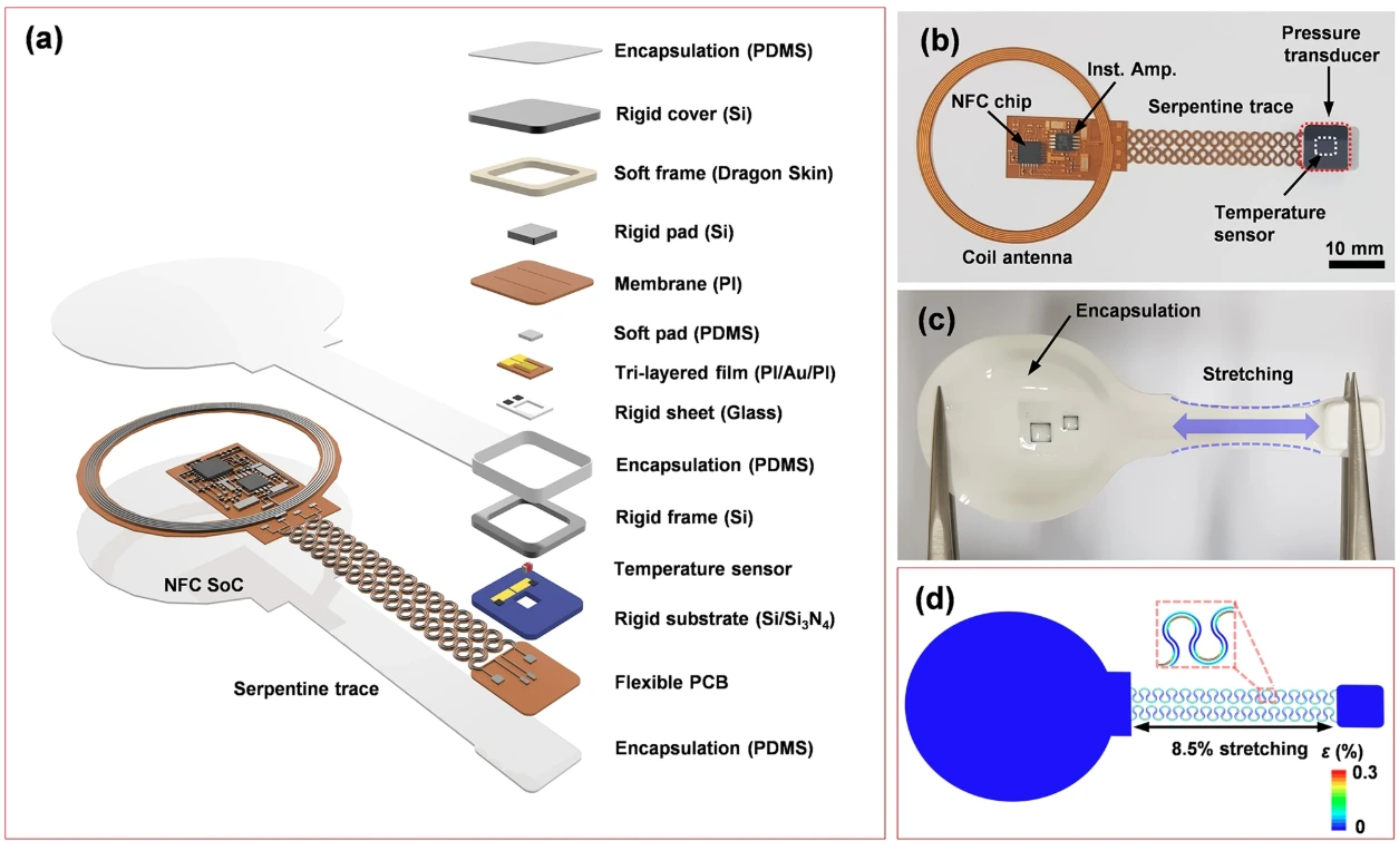
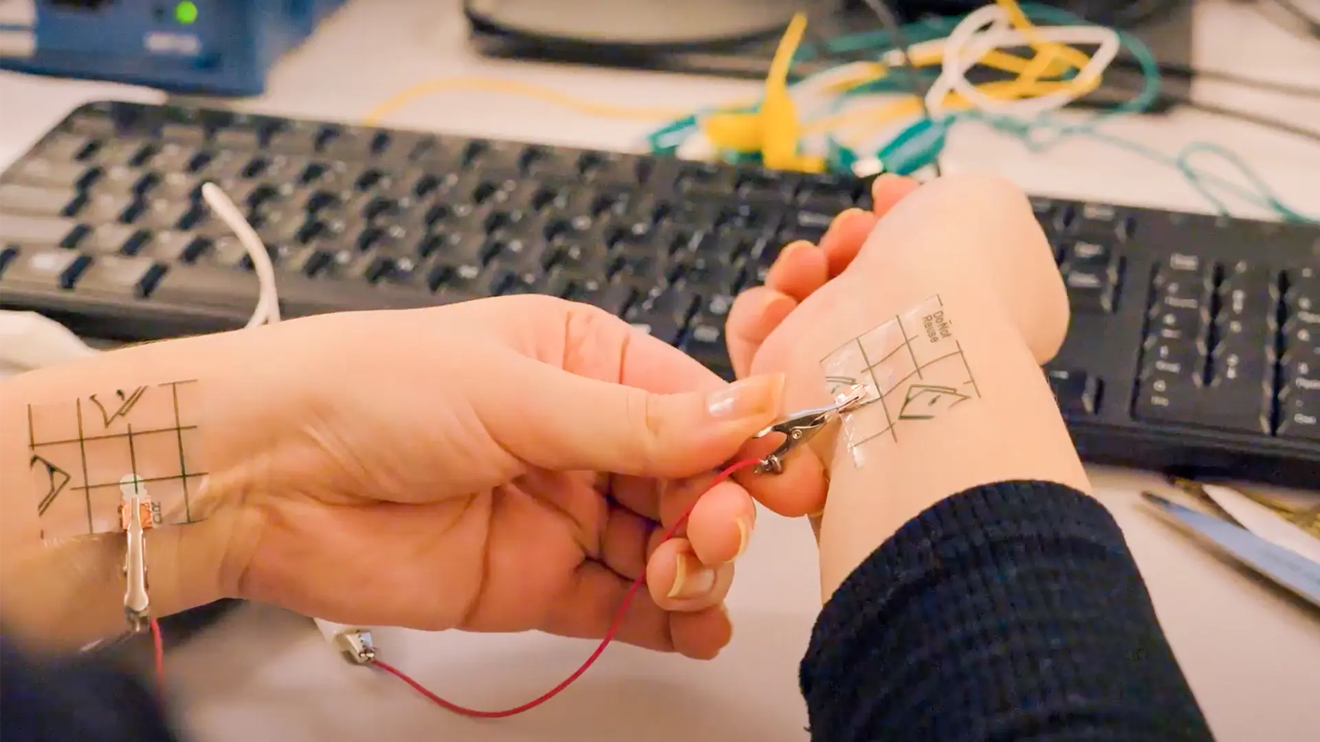
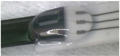
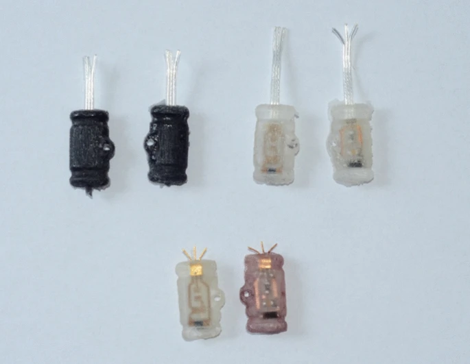
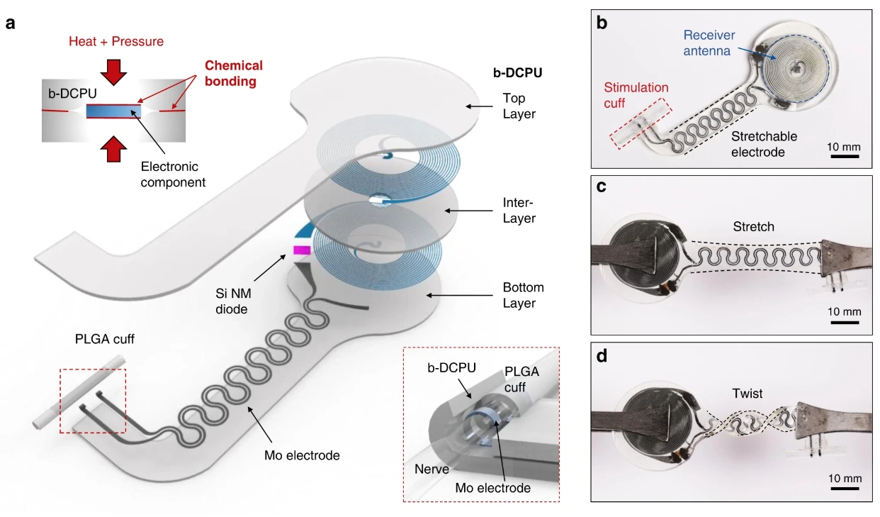
Silicones, particularly polydimethylsiloxane (PDMS), are flexible elastomers used when mechanical flexibility or biocompatibility is needed. Common in medical electronics and wearable devices, they can be applied as soft coatings, gels, or flexible encapsulants.
Pros
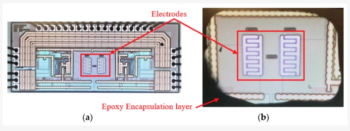
- Silicone encapsulants are soft and elastic after curing and reduce stress on sensitive components. In one study [3], a silicone encapsulant successfully protected chronically implanted PCBs, maintaining encapsulant integrity and adhesion during 30-day accelerated aging in saline.
- Silicones have excellent thermal stability and remain functional from roughly -40 °C up to 175 °C or more, a range over which they maintain consistent properties.
Cons
- Silicone encapsulation is not hermetic – moisture can slowly diffuse through, which can be problematic in very moisture-sensitive devices [4]
- Silicone doesn’t adhere as strongly to many substrates compared to epoxy, and its low surface energy makes it easy for it to “wet out” and flow into crevices, which can lead to poor adhesion if not primed.
Polyurethane
Polyurethanes (PU) are polymers formed by reacting diisocyanates with polyols, resulting in urethane linkages [5]. They strike a balance between the hardness of epoxies and the softness of silicones, offering moderate flexibility and toughness, and are useful in soft robotics, wearables, and implantables.
Pros
- Polyurethanes are semi-flexible (softer than epoxies but stiffer than silicone) and offer good electrical insulation and vibration damping. They tend to cure to a less rigid state, putting less stress on delicate parts [5].
- PU potting compounds also exhibit good adhesion [5].
Cons
- PU generally cannot withstand high temperatures as well as epoxies and silicones.
- PU is generally not as impermeable to water as epoxies. In a humid environment, a PU encapsulate is more likely to allow moisture ingress.
Conclusion
Encapsulation is a fundamental part of the electronics manufacturing process, providing protection against harsh environmental conditions like moisture, chemicals, and mechanical stress. The choice of encapsulant directly affects device reliability, making it a key design consideration for both conventional and advanced electronic systems.
Interested in learning more about electronics encapsulation? Check out these resources:
- White paper: Printing a Flexible PCB with Silver Ink on PET
- Application: Adhesive Dispensing Systems
- Blog: What Is Thermal Interface Material (TIM)?
Want to explore dispensing encapsulants with NOVA? Book a meeting to speak with one of our technical representatives.
References
[1] Inamdar, A., Driel, V., & Zhang, G. (2025). Electronics packaging materials and component-level degradation monitoring. Frontiers in Electronics, 6. https://doi.org/10.3389/felec.2025.1506112.
[2] Du, S. Baek. Y., Wang, G., & Bhattacharya, S. (2010, November 1). Design considerations of high voltage and high frequency transformer for solid state transformer application. IEEE Xplore. https://doi.org/10.1109/IECON.2010.5674991.
[3] Adam, C., M Münch, P Kleinschnittger, Barth, T., & Krautschneider, W. H. (2024). Rapid prototyping of molds for the encapsulation of electronic implants using additive manufacturing. Additive Manufacturing Meets Medicine (AMMM). https://doi.org/10.18416/AMMM.2024.24091858.
[4] Lamont, C., Grego, T., K. Nanbakhsh, A. Shah Idil, Giagka, V., A. Vanhoestenberghe, Cogan, S., & Donaldson, N. (2021). Silicone encapsulation of thin-film SiO x , SiO x N y and SiC for modern electronic medical implants: a comparative long-term ageing study. Journal of Neural Engineering, 18(5), 055003–055003. https://doi.org/10.1088/1741-2552/abf0d6.
[5] Bonomo, M., Taheri, B., Bonandini, L., Castro-Hermosa, S., Brown, T. M., Zanetti, M., Menozzi, A., Barolo, C., & Brunetti, F. (2020). Thermosetting Polyurethane Resins as Low-Cost, Easily Scalable, and Effective Oxygen and Moisture Barriers for Perovskite Solar Cells. ACS Applied Materials & Interfaces, 12(49), 54862–54875. https://doi.org/10.1021/acsami.0c17652.
Check out our Customer Stories
Take a closer look at what our customers are doing in the industry.